English
A reliable printed circuit board does not come from fabrication alone. It comes from a controlled sequence of engineering checks, material selection, circuit imaging, drilling, plating, solder mask application, component placement, soldering, and testing. If any stage is poorly managed, defects can appear later as open circuits, short circuits, soldering failures, intermittent connections, or premature product failure.
For engineers and purchasing teams, understanding the Steps in PCB Fabrication and Assembly is more than a technical exercise. It helps you evaluate manufacturers, identify cost drivers, set realistic lead times, and avoid expensive redesigns. Our recommendation is to assess the complete manufacturing flow rather than choosing a supplier based only on its bare-board price or advertised assembly speed.
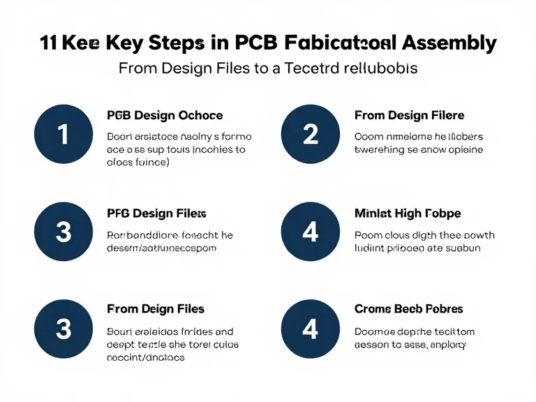
Quick Answer: What Are the Steps in PCB Fabrication and Assembly?
The main steps are: (1) PCB design and engineering review, (2) material preparation, (3) copper-clad laminate cutting and inner-layer imaging, (4) etching and inner-layer inspection, (5) lamination and drilling, (6) copper plating and outer-layer imaging, (7) solder mask, surface finish, and board profiling, (8) bare-board electrical testing and inspection, (9) component sourcing and SMT or through-hole assembly, and (10) final inspection, functional testing, and delivery.
Our practical advice: Do not treat fabrication and assembly as separate purchasing decisions unless you have a clear reason to split them. For most projects, coordinating both processes through one capable manufacturing partner makes engineering communication, quality traceability, and production scheduling easier.
PCB Fabrication vs. PCB Assembly: What Is the Difference?
PCB fabrication creates the physical printed circuit board: its insulating substrate, copper traces, conductive vias, solder mask, surface finish, and mechanical outline. PCB assembly takes that manufactured board and installs the electronic components required to make the circuit operate.
These processes are connected, but they involve different equipment, process controls, and quality checks. A bare board can pass electrical testing and still experience assembly defects if its pad design, solder mask registration, or surface finish is unsuitable for the selected components. Similarly, excellent SMT workmanship cannot compensate for a defective plated via or an incorrectly fabricated copper layer.
For a typical electronic product, the complete process starts with design data and ends with a tested PCBA. A manufacturer should be able to explain how it controls the handoff between fabrication and assembly, especially when the project includes fine-pitch components, BGA packages, controlled impedance, or multilayer structures.
Quick Summary Table: The 10 Steps in PCB Fabrication and Assembly
| Step | Process | Main Purpose | Important Quality Check |
|---|---|---|---|
| 1 | Design and engineering review | Confirm manufacturability and production data | Gerber, drill, BOM, stack-up, DFM review |
| 2 | Material preparation | Select and prepare laminate and copper materials | Material grade, thickness, copper weight |
| 3 | Inner-layer imaging | Transfer circuit patterns onto copper layers | Alignment and image accuracy |
| 4 | Etching and inspection | Remove unwanted copper and verify patterns | Trace width, spacing, shorts, opens |
| 5 | Lamination and drilling | Bond layers and create holes | Layer registration and drill position |
| 6 | Plating and outer-layer imaging | Connect layers electrically and form outer circuits | Via plating and conductor integrity |
| 7 | Solder mask and surface finish | Protect copper and prepare solderable pads | Mask registration and finish quality |
| 8 | Bare-board testing | Verify the fabricated board before assembly | Electrical continuity and isolation |
| 9 | Component assembly | Install and solder electronic components | Placement accuracy and solder quality |
| 10 | Final inspection and testing | Confirm assembled-board quality and operation | AOI, X-ray where needed, ICT or functional test |
01Step 1: PCB Design and Engineering Review
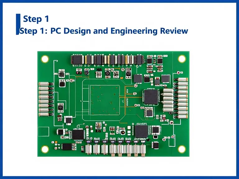
The first step is reviewing the design files before any production material is committed. This is where a manufacturer checks whether the proposed PCB can be fabricated reliably using the selected process, materials, and equipment.
Typical production data includes Gerber or other accepted manufacturing files, NC drill files, board outline, layer stack-up, fabrication notes, impedance requirements, and controlled dimensions. For assembly, the package should also include a bill of materials (BOM), centroid or pick-and-place file, assembly drawings, and component specifications.
What manufacturers should check
Trace width, copper spacing, annular rings, and minimum feature sizes.
Layer count, board thickness, copper weight, and dielectric construction.
Drill sizes, via structures, edge clearances, and board tolerances.
Component footprints, polarity markings, and assembly clearances.
Impedance requirements, thermal needs, and operating environment.
From our experience, incomplete or conflicting design files are a frequent source of avoidable delays. A board house should raise questions before production, not make undocumented assumptions and leave the customer to discover the problem during assembly.
For a new design, a PCB prototype service is useful for validating the design before committing to a larger order. We recommend a DFM review even when the design has already passed electrical simulation.
02Step 2: Material Preparation and Copper-Clad Laminate Selection
Once the design is approved, the manufacturer selects the base material. A conventional rigid PCB commonly uses copper-clad laminate, consisting of an insulating core reinforced with material such as glass fiber and coated with copper foil. Prepreg is also used in multilayer construction to bond layers together.
FR-4 is widely used because it offers a practical balance of electrical performance, mechanical strength, availability, and cost. However, it is not automatically the right material for every application. High-temperature environments, high-speed signals, RF circuits, flexible designs, and thermal-management requirements may call for different material systems.
How to choose the right PCB material
Standard electronics: FR-4 is often the most cost-effective starting point.
Higher thermal requirements: Consider a suitable high-TG material after checking the actual temperature profile and reliability target.
High-speed or RF designs: Review dielectric properties, loss characteristics, impedance control, and material consistency.
Flexible applications: Use a flexible circuit material system rather than forcing a rigid laminate into a bending application.
LED and power applications: Aluminum or other metal-core constructions may help manage heat.
For standard rigid designs, see FR4 PCB options. For elevated thermal requirements, compare the design conditions with High TG PCB materials. Do not pay for a premium laminate simply because its specification looks impressive. The material must solve a real electrical, thermal, or reliability problem.
03Step 3: Inner-Layer Imaging
For multilayer PCBs, the inner copper layers are processed before the layers are bonded together. The copper surface is cleaned and coated with a photosensitive film. A circuit image is then transferred to the film through a controlled exposure process, typically using direct imaging or an equivalent photolithographic method.
The exposed or unexposed areas are developed according to the resist system. This creates a patterned protective layer that defines which copper areas will remain after etching.
Imaging accuracy matters because the circuit pattern determines the electrical paths and clearances inside the finished board. Small registration errors can become serious when the design uses fine traces, dense routing, or tightly aligned multilayer connections.
For advanced designs, imaging capability should be evaluated alongside minimum line width and spacing, layer-to-layer registration, and the manufacturer's experience with the required stack-up. A supplier that mainly produces simple two-layer boards may not be the best choice for a dense HDI project.
04Step 4: Etching and Inner-Layer Inspection
After imaging, unwanted copper is removed through a controlled chemical etching process. The remaining copper forms the intended traces, pads, and planes. The protective resist is then stripped, exposing the finished inner-layer circuit pattern.
The manufacturer inspects the patterned layers to identify defects such as open circuits, shorts, under-etching, over-etching, and dimensional inconsistencies. Automated optical inspection (AOI) compares the actual copper pattern with the original design data.
AOI is particularly important for multilayer PCBs because inner-layer defects can become difficult or impossible to access after lamination. Finding a defect at this stage is generally less costly than discovering it after the entire board has been built.
05Step 5: Multilayer Lamination and Drilling
For multilayer boards, the prepared copper layers and bonding materials are stacked in the specified order. Heat and pressure are applied in a controlled lamination cycle to bond the layers into one solid structure. Correct stack-up design and lamination control are essential for electrical performance and mechanical reliability.
After lamination, holes are drilled according to the NC drill data. These holes may include through-holes, vias, and other mechanical features. Depending on the design, laser drilling may be used to create smaller microvias for high-density interconnect structures.
Why this stage affects reliability
Misregistration can cause poor alignment between drilled holes and internal copper pads.
Incorrect drilling conditions can create rough hole walls or damage the surrounding laminate.
Improper lamination can contribute to voids, delamination, or inconsistent dielectric thickness.
High-density designs require tighter control of via geometry and layer registration.
For standard designs, conventional mechanical drilling is usually sufficient. For dense routing and microvia structures, review whether laser-drilled PCB technology is appropriate. It is a capability to specify when the design requires it, not an upgrade every board needs.
06Step 6: Copper Plating and Outer-Layer Circuit Formation
Drilled holes must be made conductive so that the required electrical connections can pass between PCB layers. The hole walls are prepared and metallized, followed by copper plating to build up the conductive layer. This creates plated-through holes and connects the internal and external copper layers.
The outer copper layers are then patterned using imaging and etching processes similar to those used for inner layers. The final pattern forms the board's external traces, pads, and planes.
Via quality is especially important. Inadequate plating, voids, cracks, or poor hole-wall preparation can cause intermittent connections or failures during thermal cycling. These defects may not be obvious from a quick visual inspection.
For demanding applications, discuss the required copper thickness, via structure, aspect ratio, thermal reliability, and applicable qualification criteria with the manufacturer. A supplier should be able to explain how its process supports the specified board construction rather than simply confirming that it can produce the requested layer count.
07Step 7: Solder Mask, Surface Finish, and Board Profiling
Once the copper circuit pattern is complete, solder mask is applied to protect copper surfaces and reduce the risk of solder bridging during assembly. Openings are left where solder pads and other exposed features are required. Legend printing may then add component identifiers, polarity markings, logos, and other assembly information.
The exposed copper pads receive a surface finish to protect them from oxidation and provide a suitable solderable surface. Common options include lead-free HASL, ENIG, immersion silver, and OSP. The right choice depends on component pitch, storage requirements, assembly process, reliability expectations, and cost.
| Surface Finish | Typical Strength | Points to Consider | Common Application |
|---|---|---|---|
| Lead-free HASL | Established and economical | Surface may be less flat than alternatives | Many general-purpose boards |
| ENIG | Flat surface and good solderability when properly controlled | Higher cost; process quality must be managed | Fine-pitch SMT and many multilayer designs |
| Immersion Silver | Flat surface with good solderability | Requires appropriate handling and storage | Selected fine-pitch and high-frequency applications |
| OSP | Cost-effective and flat | Surface protection and storage conditions need attention | Suitable volume production applications |
After finishing, the board is routed, V-scored, or otherwise profiled to its final dimensions. Edge quality, dimensional tolerance, and panelization should be checked against the assembly requirements. A board that is difficult to fixture or separate can create problems later on an automated SMT line.
08Step 8: Bare PCB Inspection and Electrical Testing
Before components are installed, the bare PCB should pass the inspections and tests defined by the purchase specification. Visual inspection checks workmanship and observable defects. AOI can identify pattern-related issues, while electrical testing verifies that the intended connections are continuous and that unintended shorts are absent.
Flying-probe testing is often practical for prototypes and lower-volume orders because it does not require a dedicated fixture. Bed-of-nails testing uses a fixture to contact multiple test points and can be efficient for repeat production. The right method depends on the board design, volume, test coverage, and cost.
For commercial users, the key is not simply asking whether a board is tested. Ask what is tested, which netlist or test data is used, what constitutes a pass, and whether results can be traced to the production lot. If the project has special reliability requirements, define the inspection and acceptance criteria before the purchase order is released.
09Step 9: Component Sourcing and PCB Assembly
PCB assembly begins after the bare board is accepted and the components, production files, and assembly instructions are ready. The manufacturer verifies the BOM, checks component availability, prepares solder paste and stencils where required, and configures the assembly line.
For surface mount technology (SMT), solder paste is deposited onto the appropriate pads through a stencil. Automated pick-and-place equipment positions components, and the board passes through a reflow oven where the solder joints are formed according to the specified thermal profile.
Through-hole components are inserted into plated holes and soldered using an appropriate process, such as selective soldering or wave soldering. Some products use a mixed-technology process that combines SMT and through-hole components on the same board.
What to check before assembly starts
BOM accuracy: Confirm manufacturer part numbers, approved alternatives, package types, and quantities.
Component authenticity: Define sourcing requirements and traceability expectations, especially for critical parts.
Footprint compatibility: Verify that the selected component package matches the PCB land pattern.
Polarity and orientation: Confirm pin-one markings, diode direction, connector orientation, and component rotation.
Moisture-sensitive parts: Apply the required storage, floor-life, and handling controls.
Thermal process: Ensure the reflow profile is suitable for the components, solder paste, and PCB construction.
For a project using fine-pitch ICs, 0402 components, or BGA packages, assembly capability is a major supplier-selection factor. A manufacturer needs suitable equipment, process control, inspection capability, and experienced engineering support.
Why SMT PCB Assembly Is Often the Practical Choice
SMT is widely used because it supports high component density, automated placement, repeatable production, and efficient assembly at scale. It is usually the preferred process for compact consumer electronics, industrial control boards, communication equipment, and many other modern electronic products.
However, SMT is not automatically the best solution for every component. Large connectors, high mechanical-load parts, or components designed for through-hole mounting may still require through-hole assembly. The correct process is determined by the component design and product requirements.
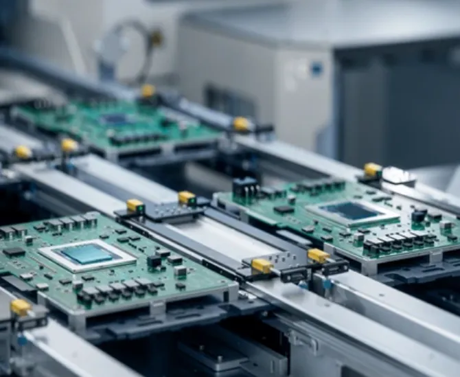
365PCB SMT PCB Assembly services support prototype through volume production, with automated SMT lines, no minimum order quantity, and assembly for components including 0402 chip parts, fine-pitch ICs, and BGA packages. The service supports lead-free RoHS and leaded soldering, with inspection processes intended to meet applicable IPC requirements. Explore SMT PCB assembly services when you need a coordinated assembly solution.
10Step 10: Final Inspection, Testing, and Delivery
After assembly, the PCBA undergoes final inspection and, where specified, electrical or functional testing. The objective is to confirm that components are correctly installed, solder joints meet the agreed acceptance criteria, and the assembled circuit performs as intended.
Common final inspection and test methods
Automated Optical Inspection (AOI): Checks visible component placement, polarity, soldering, and other observable assembly conditions.
X-ray inspection: Helps inspect hidden solder joints, including many BGA connections and other concealed terminations.
In-Circuit Test (ICT): Checks electrical characteristics and component connections using a test fixture where appropriate.
Flying-probe testing: Provides electrical test coverage without a dedicated ICT fixture, depending on the test strategy.
Functional testing: Verifies that the assembled board performs its intended functions under defined test conditions.
Visual and workmanship inspection: Checks assembly quality against the agreed workmanship and acceptance requirements.
Not every PCB needs every test method. A simple low-risk prototype may require visual inspection and basic functional verification, while a high-reliability industrial or medical application may need a more extensive test plan. The test scope should reflect the product's failure risk and contractual requirements.
Before shipment, confirm packaging, ESD protection, moisture protection where required, labeling, lot identification, and documentation. For repeat orders, retain approved BOM revisions, assembly files, test requirements, and engineering change records so that future production matches the qualified build.
PCB Fabrication and Assembly Process Comparison: What Matters at Each Stage?
The ten steps can be grouped into three manufacturing phases. Understanding the differences helps buyers identify where a supplier's capabilities are most important and where additional controls may justify their cost.
| Phase | Key Activities | Main Risk | What to Ask the Manufacturer |
|---|---|---|---|
| Engineering and preparation | DFM, material selection, stack-up, data review | Design or documentation errors carried into production | Do you provide engineering review and resolve file discrepancies before release? |
| Bare-board fabrication | Imaging, etching, lamination, drilling, plating, finishing | Layer defects, poor registration, via or surface-finish problems | Which in-process inspections and electrical tests are included? |
| Assembly and verification | Component sourcing, SMT, through-hole, inspection, testing | Wrong parts, placement defects, soldering defects, functional failures | What sourcing controls, inspection methods, and test records are available? |
For most buyers, the best supplier is not necessarily the one with the most impressive machine list. It is the one that can demonstrate control over the specific risks in your design and provide clear evidence that the finished product meets the agreed requirements.
Pros and Cons of Using an Integrated PCB Fabrication and Assembly Manufacturer
Combining fabrication and assembly under one supplier can simplify project management, but it is not always the lowest-cost choice. The decision depends on design complexity, production volume, quality requirements, and how much control your team needs over the supply chain.
| Advantages | Disadvantages |
|---|---|
| One engineering contact for fabrication and assembly questions. | Less flexibility if you want to use a specialist board fabricator or assembler separately. |
| Reduced coordination between bare-board delivery and assembly scheduling. | The supplier must genuinely have strong capability in both processes. |
| Potentially clearer responsibility when a defect occurs between fabrication and assembly. | It may be harder to compare individual process costs without a detailed quotation. |
| More consistent management of revisions, production files, and traceability. | Supplier dependence can increase if there is no qualified alternative source. |
| Can simplify prototype-to-volume production planning. | Not every integrated provider is competitive for every board technology or volume. |
Our view: Integrated manufacturing is worth considering when schedule coordination, engineering communication, and accountability are important. For highly specialized boards or very large production programs, compare integrated and split-supplier models using total landed cost, quality performance, and delivery risk rather than unit price alone.
Why Understanding the Steps in PCB Fabrication and Assembly Matters
Knowing the process gives engineering and procurement teams more control over the final result. It helps them ask specific questions instead of relying on general promises about quality or speed.
Better design-for-manufacturing decisions
When the engineering team understands material limits, drill capabilities, layer registration, and assembly constraints, it can avoid design features that add cost without improving product performance. A design review early in the project is usually cheaper than correcting a manufacturing problem after tooling or production has started.
More predictable lead times
Lead time depends on more than the number of fabrication days. Material availability, layer count, special finishes, impedance requirements, component lead times, stencil preparation, assembly complexity, and testing all affect the schedule. Understanding the production sequence makes it easier to identify the real bottleneck.
Improved quality accountability
When each process has defined inspection criteria, defects can be traced to the relevant manufacturing stage. This is particularly important for products with repeat production, field-service obligations, or strict customer acceptance requirements.
More informed cost control
Material upgrades, extra inspection, special drilling, and advanced assembly methods can all add cost. They should be selected to address a known design or reliability requirement. The objective is not to buy the most expensive process; it is to achieve the required performance with an appropriate level of manufacturing control.
Common Mistakes in PCB Fabrication and Assembly
1. Releasing incomplete or inconsistent production files
Outdated Gerber files, mismatched drill data, missing stack-up information, and incomplete assembly drawings can create production delays or incorrect builds. Use a controlled revision package and make sure the manufacturer confirms which revision is approved.
2. Choosing materials based only on price
A lower-cost laminate may not satisfy the board's thermal, electrical, or mechanical requirements. Specify material performance according to the real operating conditions rather than selecting by price alone.
3. Ignoring assembly requirements during PCB design
Footprint errors, inadequate component spacing, poor fiducial placement, and inaccessible test points can complicate assembly. Include the assembly manufacturer in the design review when practical.
4. Treating all surface finishes as interchangeable
Different finishes have different characteristics, costs, storage requirements, and suitability for fine-pitch assembly. Confirm the finish with the assembler before finalizing the fabrication specification.
5. Skipping electrical testing to reduce cost
Testing decisions should be based on risk and production volume. Removing an essential bare-board electrical test may reduce the initial quote but increase the risk of paying for assembly on defective boards.
6. Assuming AOI proves the board is fully functional
AOI identifies visible defects within its inspection capability. It does not replace electrical testing or functional verification. Use the right combination of inspection and testing for the product.
7. Failing to control component substitutions
Substituting a component based only on a similar part number or package can create electrical, thermal, firmware, or regulatory problems. Require customer approval for substitutions that affect the approved design or BOM.
How to Choose a PCB Fabrication and Assembly Manufacturer
Choosing a PCB supplier should start with the technical requirements of the product, not a generic comparison of advertised capabilities. A manufacturer may be excellent at standard rigid boards but less suitable for flexible circuits, HDI, high-TG materials, or fine-pitch assembly.
1. Match manufacturing capability to the board design
Check layer count, board thickness, copper weight, minimum trace and spacing, drill sizes, via structures, material options, and impedance capability. If your product requires flexible or rigid-flex construction, confirm that the supplier has relevant production experience. You can compare options such as FPC PCB and rigid-flex PCB against the mechanical requirements of the design.
2. Review the assembly line and component range
Ask about SMT line configuration, placement capability, stencil printing, reflow control, through-hole processing, and support for fine-pitch or BGA components. Confirm whether the supplier can handle your actual component packages rather than relying on a general statement that it offers SMT assembly.
3. Ask for quality procedures and acceptance criteria
Discuss the applicable IPC standards, inspection stages, electrical test methods, defect handling, and traceability. The purchase specification should identify the acceptance class and any additional customer requirements. Avoid assuming that the phrase "IPC compliant" automatically defines every inspection detail.
4. Evaluate component sourcing controls
For turnkey assembly, ask whether components are sourced from authorized channels, how substitutions are approved, and what traceability documents are available. Counterfeit or incorrectly specified components can undermine an otherwise well-controlled assembly process.
5. Compare total project cost, not just the PCB unit price
A useful quotation should separate or clearly explain board fabrication, tooling or setup, stencil, components, assembly, testing, packaging, and shipping. Consider engineering support and the cost of managing multiple suppliers. The cheapest bare-board quote may not result in the lowest finished-PCBA cost.
6. Confirm prototype and production support
For a new product, the manufacturer should be able to support engineering samples, prototype builds, design changes, and later production scaling. A supplier that can maintain revision control from prototype to volume production can reduce the risk of repeated setup work and inconsistent builds.
PCB Fabrication and Assembly Cost: Where Should You Spend More?
There is no single price for PCB fabrication and assembly. Cost is influenced by board dimensions, layer count, material, copper thickness, minimum features, via technology, surface finish, order quantity, component count, package complexity, component availability, testing, and delivery requirements.
For beginners and early-stage product teams, the best cost-control strategy is to keep the design manufacturable and avoid unnecessary complexity. A standard FR-4 multilayer board may be sufficient where a specialized laminate or HDI construction offers no meaningful product benefit. Likewise, not every assembly requires expensive X-ray inspection or a dedicated functional test fixture.
For commercial users, the calculation should include the cost of defects, rework, schedule delays, and field returns. Spending more on a controlled process can be justified when a failure would interrupt production or damage customer confidence.
| Cost Area | When Spending More Is Justified | Where to Avoid Unnecessary Cost |
|---|---|---|
| PCB material | High temperature, signal integrity, flexibility, or thermal requirements demand it. | Do not specify premium materials without a measurable design need. |
| Layer count and HDI | Routing density, size, or electrical performance requires advanced construction. | Revisit component placement and routing before increasing complexity. |
| Surface finish | Fine-pitch components, storage conditions, or assembly requirements justify a specific finish. | Do not select a costly finish simply because it sounds more advanced. |
| Inspection and testing | High-risk products or hidden solder joints require additional verification. | Align test coverage with product risk and acceptance requirements. |
| Assembly process | Fine-pitch, BGA, mixed-technology, or high-volume production needs specialized controls. | Do not pay for advanced processes that the component set does not require. |
We recommend requesting a prototype quotation and a production-volume quotation where possible. This reveals which costs are fixed setup expenses and which decrease with quantity. It also helps the team understand whether a design change could reduce long-term production costs.
Expert Recommendation: How to Manage the Complete PCB Manufacturing Process
Our recommendation is to treat PCB fabrication and assembly as one connected engineering workflow, even if different suppliers perform the two operations. The design, materials, bare-board acceptance criteria, component selection, assembly files, and test plan must all support the same product requirements.
For a first prototype, prioritize a thorough DFM review, correct material selection, basic electrical verification, and a functional test that checks the product's essential behavior. Do not spend heavily on advanced manufacturing options until the design or operating conditions justify them.
For repeat commercial production, put more emphasis on process consistency, component traceability, documented inspection criteria, controlled engineering changes, and production records. A supplier should be able to explain how it prevents an approved prototype from drifting into an undocumented production variation.
For heavy-duty applications or products where field failure is expensive, define the reliability and verification requirements before requesting quotations. Consider whether the board needs high-TG material, controlled impedance, specialized via structures, conformal coating, additional inspection, or extended testing. These should be engineering decisions, not assumptions added to every order.
Looking for a PCB Fabrication and Assembly Partner?
365PCB provides PCB manufacturing and SMT PCB assembly support for projects ranging from prototypes to production orders. When evaluating a supplier, share your board files, stack-up requirements, BOM, assembly drawings, and testing expectations so the manufacturing team can assess the complete project.
Learn more about 365PCB SMT PCB Assembly services and discuss the fabrication and assembly requirements for your next project.
Frequently Asked Questions About the Steps in PCB Fabrication and Assembly
1. What are the main steps in PCB fabrication and assembly?
The main steps include design review, material preparation, inner-layer imaging, etching, lamination, drilling, copper plating, outer-layer formation, solder mask and surface finishing, bare-board testing, component assembly, and final inspection. The exact process varies according to board type, layer count, and assembly technology.
2. What is the difference between PCB fabrication and PCB assembly?
PCB fabrication produces the bare circuit board, including copper traces, vias, substrate, solder mask, and surface finish. PCB assembly installs and solders electronic components onto the fabricated board to create a functional PCBA.
3. How long does PCB fabrication and assembly take?
Lead time depends on board complexity, layer count, material availability, special processes, component sourcing, assembly quantity, and testing requirements. A simple prototype can move faster than a complex multilayer board with scarce components or specialized inspection needs. Ask for separate fabrication, component procurement, assembly, and testing timelines.
4. What materials are commonly used in PCB fabrication?
FR-4 is widely used for rigid PCBs. Other options include high-TG laminates, specialized high-frequency materials, flexible circuit materials, and metal-core constructions. The correct material depends on electrical performance, operating temperature, mechanical requirements, and product environment.
5. Why is copper plating important in PCB manufacturing?
Copper plating creates conductive connections inside drilled holes, allowing signals and power to travel between PCB layers. Poor plating quality can lead to unreliable vias, intermittent connections, and failures during product operation or thermal cycling.
6. What is SMT PCB assembly?
SMT PCB assembly is a process in which surface-mount components are placed directly onto PCB pads. Solder paste is printed onto the pads, components are positioned by automated equipment, and the board passes through a reflow process to form solder joints. SMT supports compact layouts and efficient automated production.
7. Is AOI testing enough for a finished PCBA?
No. AOI checks visible assembly features, but it cannot verify every electrical or functional requirement. Depending on the product, a complete verification plan may also include X-ray inspection, ICT, flying-probe testing, and functional testing.
8. Which IPC standards are relevant to PCB fabrication and assembly?
Relevant standards depend on the product and contractual requirements. IPC-2221 covers general printed-board design, IPC J-STD-001 addresses requirements for soldered electrical and electronic assemblies, and IPC-A-610 provides acceptability criteria for electronic assemblies. The applicable revisions and product class should be agreed between the customer and manufacturer.
9. Should I choose a manufacturer that offers both PCB fabrication and assembly?
An integrated supplier can simplify engineering communication, scheduling, and responsibility for quality issues across the manufacturing flow. It is a strong option for prototypes and many commercial projects. However, compare its specific fabrication and assembly capabilities with your design requirements rather than assuming every integrated supplier is equally qualified.
10. What files are needed for a PCB fabrication and assembly quotation?
For fabrication, provide the Gerber or accepted manufacturing data, NC drill files, board outline, stack-up, material and thickness requirements, copper weight, surface finish, and fabrication notes. For assembly, provide the BOM, centroid or pick-and-place file, assembly drawings, component specifications, and any special process or test requirements.
References and Industry Standards
The following industry references provide guidance for PCB design, soldering process requirements, and electronic assembly acceptance. Always confirm the applicable revision and contractual requirements for your specific product.
IPC-2221C: Generic Standard on Printed Board Design — IPC's foundational design standard covering general requirements for printed boards and interconnecting structures.
IPC J-STD-001: Requirements for Soldered Electrical and Electronic Assemblies — Describes materials, methods, process requirements, and acceptance criteria for soldered electronic assemblies. Confirm the applicable current revision with IPC.
IPC-A-610J: Acceptability of Electronic Assemblies — Provides visual acceptability requirements for electronic assemblies and supports consistent workmanship evaluation.