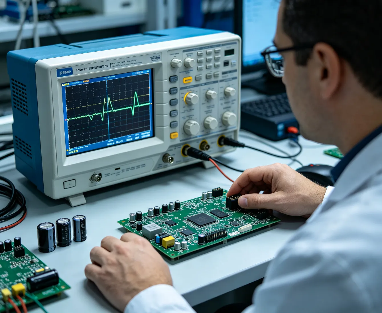
Start With the Load Requirement
Before choosing decoupling capacitors, define:
0.8 V?
1.0 V?
1.8 V?
3.3 V?
How much static regulator / IR-drop error is allowed?
How much dynamic voltage variation can the load tolerate?
What is the sustained load?
How quickly can current change?
At what time scales does the load demand energy?
Power Integrity Begins With the Silicon Requirement.
Voltage Margin Is a Budget
A load may allow only a finite voltage range.
Conceptually:
must absorb contributions from:
VRM Accuracy
DC IR Drop
Transient Droop
Ripple
Noise
Temperature / Variation
Every Error Mechanism Spends Voltage Margin.
This is directly analogous to:
in Signal Integrity.
DC Margin vs AC Margin
It is useful to separate:
regulator accuracy
copper drop
connector drop
steady-state distribution
from:
transient response
resonances
switching noise
dynamic load
A Rail Can Pass DC Regulation and Still Fail Power Integrity.
Current Profile
Do not design only from:
Typical current = 15 A.
A processor or FPGA may dynamically move between:
in extremely short time intervals.
Average Current Determines Energy.
Current Change Determines Power Integrity.
Current Step
A useful engineering abstraction is:
ΔI
the expected transient change in current.
For example:
is a 20 A current step.
The PDN must supply that additional current while the regulator and other energy sources respond.
The Faster ΔI Happens, the More Local the Energy Source Must Become.
Target Impedance
The central PI concept is:
A common first-order relationship is:
For example, tighter allowable ripple or larger current step drives required PDN impedance lower.
AMD's June 2026 Versal design guide continues to use this exact engineering principle, calculating target impedance from ripple tolerance and step-current demand and recommending full board-level PDN simulation for verification.
Voltage Margin Divided by Current Demand Becomes an Impedance Requirement.
Why Target Impedance Is Powerful
Instead of asking:
How many 100 nF capacitors?
the engineer asks:
What maximum impedance can the load tolerate across the frequency range where the PCB PDN must support it?
That transforms PI from:
component recipes
into:
network engineering.
PDN Impedance vs Frequency
The PDN impedance can be plotted:
The objective is generally to control problematic peaks and maintain acceptable impedance over the required bandwidth.
Intel's FPGA board-design methodology similarly describes keeping effective rail impedance below the target value from low frequencies through the required decoupling range.
Power Integrity Is a Frequency-Domain Problem.
Why Frequency Matters
A current transient contains many frequency components.
Slow load changes may be supported primarily by:
Faster events may rely increasingly on:
Different Parts of the PDN Supply Different Parts of the Frequency Spectrum.
The PDN Frequency Hierarchy
Conceptually:
Input source / main regulator.
VRM + bulk capacitance.
Board decoupling.
Package / closely mounted capacitance.
On-die structures.
No Single Capacitor Supplies Every Frequency.
The Regulator Is Part of the PDN
The VRM contributes:
output impedance
control-loop response
switching behavior
output capacitance
The PDN Does Not Begin at the Decoupling Capacitor.
It begins at the power-conversion system.
VRM Output Impedance
A regulator cannot maintain zero output impedance at every frequency.
At lower frequencies its feedback loop can actively regulate.
As frequency rises:
The Control Loop Eventually Becomes Too Slow.
Local stored energy must then support the load.
VRM Control Bandwidth
The regulator control loop responds only within a finite bandwidth.
A CPU current event occurring much faster than that loop cannot wait for feedback correction.
The Regulator Cannot Supply Energy Before Its Control Loop Knows the Load Changed.
Control-Loop Stability
The regulator and external network form a feedback system.
Its stability can depend on:
output capacitor
load
input network
The VRM and the PDN Must Not Be Designed as Completely Independent Systems.
VRM + Decoupling Interaction
An apparently excellent bank of capacitors can alter:
output impedance
resonances
control behavior.
More Capacitance Can Change the System You Are Trying to Stabilize.
Bulk Capacitance
Bulk capacitors support relatively slower, larger-energy transients.
They may sit near:
major load
board power entry.
Bulk Capacitance Stores Energy.
It Does Not Automatically Solve High-Frequency Power Integrity.
MLCC Decoupling
Ceramic capacitors provide low impedance across useful higher-frequency ranges.
But the real capacitor is:
not an ideal C.
Every Decoupling Capacitor Is an RLC Network.
ESR
Equivalent Series Resistance influences:
minimum impedance
resonance damping.
Extremely low ESR is not universally beneficial because low-loss networks can produce stronger high-Q resonances.
Some Resistance Can Be Useful Damping.
ESL
Equivalent Series Inductance limits high-frequency effectiveness.
Above self-resonance:
The Capacitor Becomes Increasingly Inductive.
This is why placing a huge nominal capacitor far from the load does not automatically make it useful at high frequency.
Self-Resonant Frequency
At the capacitor's self-resonant frequency:
capacitive reactance
and
inductive reactance
approximately cancel.
The component reaches its lowest impedance region.
Above this:
It Behaves More Like an Inductor Than a Capacitor.
Mounting Inductance
The effective inductance includes more than the component.
It also includes:
Pad
Trace
Via
Plane Connection
The PCB Is Part of the Decoupling Capacitor.
Capacitor Package Size
Smaller packages can often provide lower mounting/parasitic inductance.
But:
capacitance
voltage derating
assembly
cost
also matter.
Small Package Can Improve High-Frequency Behavior — but It Is Not a Universal Optimization.
DC Bias
MLCC effective capacitance can fall significantly under applied DC voltage depending on dielectric and construction.
Therefore:
Nominal Capacitance Is Not Necessarily In-Circuit Capacitance.
PDN models should use realistic effective values where performance demands it.
Temperature Dependence
Capacitance and other electrical characteristics can vary with temperature.
The PDN at Room Temperature Is Only One Operating Point.
Aging
Some ceramic dielectrics experience capacitance change with time.
For tight-margin products:
Component Aging Can Become PDN Variation.
Capacitor Tolerance
A:
±20% capacitor
means the PDN contains a distribution of capacitance values.
Nominal Capacitor Lists Do Not Describe Production PDNs Exactly.
Decoupling Is Not “One of Every Value”
An old heuristic is:
100 µF + 10 µF + 1 µF + 0.1 µF + 0.01 µF.
That can create unexpected resonances.
Modern flat-impedance design instead models the combined network and selects components to achieve controlled impedance with appropriate damping. Keysight explicitly recommends flat-impedance optimization rather than blindly increasing capacitor count.
A Pretty Logarithmic Capacitor Series Is Not a PDN Design.
Anti-Resonance
When different capacitors interact through inductance, the network can create:
where impedance becomes much higher than expected.
More Capacitors Can Sometimes Create More Impedance at the Wrong Frequency.
This is one of the most important PI concepts.
High-Q Resonance
A low-loss RLC network can resonate strongly.
A fast load event can excite that resonance.
The result can be:
voltage ringing
droop
overshoot
The PDN Can Ring Just Like a Signal Channel.
Flat Impedance
One advanced design objective is a relatively:
instead of deep valleys and large peaks.
Keysight's PI methodology emphasizes flat target impedance partly because high-Q impedance peaks can create large transient voltage response even when some individual frequencies look excellent.
Minimum Impedance Is Not the Goal.
Controlled Impedance Is.
Damping
Resonances can be controlled through:
component ESR
network architecture
deliberate damping where justified
A Perfectly Lossless PDN Would Not Necessarily Be a Stable Practical PDN.
Plane Capacitance
Closely spaced:
and
form distributed capacitance.
This capacitance can support higher-frequency current.
PCB Stack-Up Can Become a Distributed Capacitor.
Plane Spacing
Reducing separation between power and ground planes:
increases plane capacitance
reduces loop inductance
Z-Axis Geometry Is Part of Power Integrity.
Plane Pair Architecture
A stack-up can intentionally place certain critical power/ground planes close together.
But this must balance:
routing
fabrication
dielectric thickness
voltage
Stack-Up Is PDN Architecture.
Plane Spreading Inductance
Current traveling laterally through planes encounters inductive impedance.
As distance increases:
The Load Becomes Electrically Further From the Energy Source.
This is one reason capacitor placement matters.
Spreading Inductance
A capacitor 50 mm away from a high-current BGA may have excellent component ESL but poor effective high-frequency connection because current must spread through the plane system.
Electrical Distance Is Not Just Trace Length.
Plane Resonances
Large plane structures can support electromagnetic cavity resonances.
At sufficiently high frequency, power/ground planes no longer behave as ideal equipotential conductors.
The PCB Power Plane Can Become a Resonant Electromagnetic Structure.
Cavity Modes
Plane dimensions and dielectric properties establish resonant modes.
These can influence:
coupling between regions.
Board Dimensions Can Become Frequency-Domain Power Parameters.
Edge Effects
Plane fields can interact with board edges.
In some architectures, this may contribute to electromagnetic radiation or coupling.
Power Integrity and EMC Meet in the Plane Structure.
BGA Power Delivery
Large CPUs, GPUs, FPGAs and SoCs may contain:
many power balls
many ground balls
The BGA itself therefore becomes a major part of the power-delivery geometry.
A BGA Is a Vertical Power-Distribution Structure.
Power/Ground Ball Distribution
The number and physical arrangement of power and ground balls influences:
current distribution
inductance
package connection
Pinout Is Part of PDN Design.
BGA Via Arrays
Each ball-to-plane transition adds:
resistance
inductance.
Large via arrays create a distributed network.
BGA Power Delivery Should Be Evaluated as an Array — Not One Via Multiplied by N.
Shared Current Paths
If too much current is forced through only a small subset of vias:
voltage drop
heating
can increase.
The Current Follows Impedance — Not the Designer's Intentions.
Via Current Distribution
Parallel vias do not necessarily carry perfectly equal current.
Geometry matters:
distance
plane connection
source position
Ten Vias Do Not Automatically Equal Ten Times One-Via Capacity.
Power Via Resistance
At high current, small resistance matters.
1 mΩ × 50 A = 50 mV.
On a:
0.8 V core rail
that is a significant voltage fraction.
Milliohms Become Voltage Margin.
DC IR Drop
Power planes and vias have finite DC resistance.
Conceptually:
At tens or hundreds of amperes, tiny resistance becomes significant.
DC Power Integrity Is Geometry Too.
DC and AC PI Are Different
focuses on:
resistance
current density
steady-state voltage drop.
focuses on:
impedance
inductance
capacitance
transient response.
A Complete PDN Must Pass Both.
Current-Density Analysis
A wide plane may contain:
narrow neckdowns
voids
via bottlenecks.
Those local structures can carry much higher current density.
The Weakest Copper Geometry Can Define the Rail.
Copper Thickness
Increasing copper thickness can reduce DC resistance.
But it also affects:
impedance geometry
etch capability
Power Copper Is a Manufacturing Decision.
Current Carrying Standards Context
IPC-2221C remains the current generic PCB design standard released in late 2023. IPC's own revision table, however, now lists the older IPC-2152 current-carrying-capacity document as no longer maintained. For advanced high-current designs, it is therefore more professional to combine applicable current standards/guidance with actual thermal analysis, finished-copper geometry, environment and fabricator capability rather than present one legacy chart as universal truth.
Current Capacity Is Electrical + Thermal + Geometric.
Power Plane Neckdowns
A large plane feeding a BGA may narrow around:
via fields
keep-outs
routing.
A Large Copper Area Is Irrelevant if the Current Must Pass Through a Narrow Bottleneck.
Plane Voids
Clearances around:
signal vias
mounting holes
connectors
can fragment power paths.
Every Void Redirects Current.
Via Antipads in Power Planes
Dense signal-via fields can remove significant copper from adjacent planes.
High-Speed Escape Can Damage Power Integrity if Power Geometry Is Ignored.
This is a classic:
SI + PI Co-Design Problem.
Split Power Planes
Multiple rails may share one physical layer.
Split geometry can produce:
narrow paths
return issues
coupling.
Plane Utilization Is a Two-Dimensional Current-Flow Problem.
Remote Sense
High-current regulators may support remote sensing.
Instead of regulating voltage at the VRM pins:
Sense the Voltage at the Load.
AMD's current Versal PCB guide explicitly includes planar-resistance and remote-voltage-sense routing as part of power-system design.
Remote-Sense Routing
Sense traces should represent:
actual load voltage
without carrying significant power current.
Measurement Path and Power Path Should Be Different Where Precision Requires It.
Kelvin Sensing
This is the same fundamental principle used in precision current measurement:
Measure at the Point of Interest — Not Through the Voltage Drop You Are Trying to Measure.
Load-Line / Droop Concepts
Some processors deliberately use controlled voltage droop versus load.
Why?
Because trying to maintain perfectly constant voltage during massive current transitions may create excessive overshoot when the load suddenly decreases.
Controlled Droop Can Increase Dynamic Margin.
Static Voltage Is Not Always the Optimal Goal
The best power rail may intentionally change slightly with load if that improves overall transient behavior.
Power Integrity Is About Staying Inside the Operating Window — Not Forcing One Exact Voltage Forever.
Load Release
Engineers often focus on:
current step up.
But:
current step down
can create:
Voltage Overshoot.
The energy stored in inductive paths still needs somewhere to go.
Overshoot
When a heavy load disappears rapidly, stored energy can temporarily raise voltage.
Transient Validation Must Test Both Load Application and Load Removal.
Undershoot
When a load appears rapidly, local energy sources supply the initial current.
If PDN impedance is too high:
Voltage Droops.
Time-Domain Droop
A transient waveform can reveal:
immediate inductive drop
capacitor discharge
ringing
Different Parts of the Waveform Reveal Different Parts of the PDN.
First-Nanosecond Response
The regulator is far too slow to respond to the earliest part of an ultra-fast load event.
That energy comes from:
The Closest Electrical Energy Storage.
Ultimately including package/on-die capacitance.
Mid-Time Response
As the event continues:
local MLCC
plane capacitance
play increasingly important roles.
Longer-Time Response
Eventually:
bulk capacitance
take control.
PDN Design Is an Energy Handoff Across Time Scales.
Package PDN
The semiconductor package contains:
planes
bumps
vias
decoupling
and other power structures.
PCB PI Stops at the BGA Ball Only in the CAD Tool.
Electrically, the system continues into the package.
Package Inductance
Package interconnect introduces inductance.
At high current/edge rate:
Package Inductance Can Dominate High-Frequency Power Delivery.
Package Capacitance
Advanced packages may integrate capacitance closer to silicon.
This can support higher-frequency transient current than board-level capacitors.
Move Energy Storage Closer as the Required Response Gets Faster.
On-Die Capacitance
The final high-frequency energy reservoir is physically inside the silicon.
The PDN Ends at the Transistor.
Not at the PCB.
PCB + Package Co-Simulation
When margins are tight, a realistic PDN may combine:
Device Model.
AMD's current 2026 guidance explicitly recommends full board-level PDN simulation and provides platform-specific PDN models for this purpose.
Model the Network the Silicon Actually Sees.
Device-Specific PDN
A universal capacitor recipe is especially problematic for FPGAs.
Two customers can use the same FPGA with completely different:
utilization
clocks
transceivers
and therefore very different power dynamics.
AMD explicitly notes this fundamental point in its current FPGA design methodology.
The Chip Part Number Does Not Fully Define the Load.
The Application Does.
FPGA Power Integrity
FPGA PDN design may need to support:
Core
I/O Banks
Transceivers
Memory Interfaces
PLL / Analog Rails
with different noise/current characteristics.
One FPGA Is Several Different Power Systems.
FPGA Dynamic Current
Changing FPGA logic utilization can change:
current
switching spectrum
rail requirements.
Firmware / Bitstream Can Change Power Integrity Without Changing the PCB.
This is an extremely important concept.
CPU Power Integrity
Modern CPUs can switch huge numbers of transistors rapidly.
The current profile depends on:
workload
frequency
voltage
power management
Software Can Become a PDN Load Generator.
GPU / AI Accelerator PI
AI accelerators combine:
very high compute activity
high memory bandwidth
large current transients.
This makes PI especially important.
AI Compute Is a Power-Delivery Problem as Well as a Compute Problem.
AI Server Boards
AI server boards may simultaneously contain:
GPUs / accelerators
CPUs
DDR / HBM interfaces
PCIe / CXL
networking
enormous DC power delivery.
SI, PI, Thermal and Mechanical Architecture Must Converge.
High-Current Low-Voltage Rails
As processor voltage decreases while current rises:
Target Impedance Becomes Extremely Small.
Example conceptually:
=
More Difficult PDN.
This is one reason modern PI becomes a milliohm engineering problem.
Milliohm-Level Engineering
Rohde & Schwarz notes that PCB PDNs commonly require impedance in the milliohm range and that transient current spectra can extend toward hundreds of MHz, where PCB interconnect parasitics become active parts of the network.
At Milliohms, Every Connection Matters.
DDR Power Integrity
Memory requires clean:
power
ground
references.
Poor PI can produce:
threshold movement
timing loss
reference modulation.
DDR Signal Integrity Is Incomplete Without DDR Power Integrity.
VREF Integrity
Memory/reference voltages may set receiver thresholds.
Noise on VREF can directly change:
The Decision Boundary.
Digital Memory Contains Precision Analog Nodes.
SerDes Power Integrity
High-speed transceivers contain:
analog front ends.
Supply noise can appear as:
Jitter.
PDN-Induced Jitter
If supply noise modulates:
oscillator
transmitter driver
then voltage noise becomes:
Timing Noise.
Power Integrity Can Become Signal Integrity.
PLL Rails
PLL rails often deserve special noise analysis.
A rail can be within:
±3% DC
and still have problematic spectral content.
Voltage Tolerance Alone Does Not Define Rail Quality.
Spectral Power Noise
A rail should sometimes be evaluated as:
Noise vs Frequency.
Because the load may be particularly sensitive at specific frequencies.
RF Power Integrity
In RF systems, supply noise can become:
phase noise
spurs
receiver desense.
Power Noise Can Become RF Spectrum.
ADC Power Integrity
ADC supplies/references can convert supply disturbances into:
spurs
measurement error.
A Digitally Correct Rail Can Still Be an Analog Failure.
Mixed-Signal PI
One board may contain:
all using nominally similar voltages.
But each load has different noise sensitivity.
Same Voltage Does Not Mean Same PDN Requirement.
Rail Isolation
Sensitive rails may use:
dedicated regulators
filters
ferrite structures
where justified.
But adding filters can create:
resonance
voltage drop
control interaction.
Isolation Networks Must Be Modeled as PDNs Too.
Ferrite Beads
Ferrite beads are frequency-dependent lossy impedance components.
They can help suppress noise in some architectures.
But combined with capacitors they can form:
Resonant Networks.
“Add a Ferrite” Is Not a Complete PI Strategy.
LC Filters
An LC filter can reduce switching noise.
But low damping can create:
impedance peaks
regulator interaction.
Filters Remove Noise Only When the Network Remains Stable.
Shared Regulators
Multiple loads can share one regulator.
This reduces:
area
but introduces coupling.
One Load's Current Transient Can Become Another Load's Supply Noise.
Rail Merging
When compatible rails are merged, engineering should evaluate:
voltage tolerance
load dynamics
noise sensitivity
startup.
Intel's current Agilex 5 PDN guidelines explicitly include rail-merger and combined-rail considerations as part of device power architecture.
Shared Voltage Does Not Automatically Mean Shared Power Architecture.
Cross-Domain Coupling
A CPU transient can potentially influence:
analog
through shared power impedance.
Shared PDN Impedance Creates Electrical Communication Between Loads.
Power Rail Partitioning
Partition rails where:
noise
current
sequencing
fault containment
justify it.
More Rails Increase Complexity.
Fewer Rails Increase Coupling.
Architecture is a trade-off.
Ground Integrity
Power delivery requires:
power
and:
return current.
Power Integrity Is Power + Ground Integrity.
Ground Plane Impedance
Ground is not an ideal zero-voltage node.
It has:
resistance
inductance
resonances.
“Ground” Is a Distributed Electrical Structure.
Ground Bounce
Fast current change through shared inductance produces transient ground voltage.
This can affect:
logic thresholds
SerDes.
Reference Movement Is Signal Movement.
Simultaneous Switching Noise
Large digital banks switching simultaneously create:
transient current
ground/reference movement.
The Data Pattern Can Excite the PDN.
100 — SSN + PI
Signal activity and PDN behavior are coupled.
This becomes particularly significant in:
memory
wide parallel buses.
Digital Function Can Become Power-Spectrum Excitation.
101 — Current Return Through Planes
Power current flows through defined geometric paths.
Plane cuts and bottlenecks can force current to spread.
Power Does Not Teleport Across a Plane.
102 — Power / Ground Via Pairing
Low-inductance current delivery often benefits from short, closely related:
power
and
ground
connections.
Supply and Return Path Should Be Engineered Together.
103 — Loop Inductance
The relevant inductance is not simply:
power-via inductance.
It is strongly influenced by the complete:
Power + Return Loop.
104 — Decoupling Loop
A local decoupling path is:
Minimize the Complete Current Loop.
105 — Capacitor Orientation
Pad orientation and via location can change loop inductance.
Rotating a Capacitor Can Change Its High-Frequency Effectiveness.
106 — Via-in-Pad Decoupling
For demanding BGAs, via-in-pad or very close vias may reduce interconnect inductance.
But this must be balanced with:
fabrication
assembly
cost.
Buy Lower Inductance Only Where the Rail Needs It.
107 — Backside Capacitors
Decoupling placed beneath a BGA may provide short connection paths in suitable mechanical architectures.
But:
board thickness
vias
component clearance
still matter.
Physical Distance to the Load Is a High-Frequency Variable.
108 — Top-Side vs Bottom-Side Decoupling
The best side is determined by the actual:
via
plane
stack-up geometry.
“Place on Bottom” Is Not a Universal PI Rule.
109 — Plane-Pair Inductance
Closely coupled power/ground planes reduce inductive loop area.
This can improve:
high-frequency delivery
plane capacitance.
Thin Dielectric Can Be a PI Design Resource.
110 — Stack-Up Optimization for PI
A high-performance stack-up simultaneously manages:
and:
PI Plane Pairs.
Stack-Up Must Serve Both Signals and Power.
111 — SI vs PI Layer Competition
Signal layers want nearby ground references.
Power architecture wants:
low-inductance plane relationships.
Routing density wants more signal layers.
Stack-Up Is a Multi-Disciplinary Resource Allocation Problem.
112 — Decoupling Optimization
The goal is not necessarily:
Maximum Capacitor Count.
It is:
Minimum Practical Network That Meets the Impedance Requirement With Adequate Margin.
This can reduce:
cost
board area
solder joints.
Keysight specifically notes that flat-impedance optimization can reduce capacitor count while avoiding high-Q resonances.
113 — Capacitor Count vs Reliability
Every component introduces:
procurement
assembly
solder-joint
lifecycle
complexity.
Over-Decoupling Can Be an Engineering Cost.
114 — Optimization by Impedance
Compare capacitor combinations by:
instead of:
total µF.
Total Capacitance Is Not a PDN Performance Metric.
115 — Effective Capacitance
A 100 µF bank whose high-frequency path has excessive inductance may contribute little where the silicon needs it.
Useful Capacitance Is Frequency- and Geometry-Dependent.
116 — Capacitor Location Optimization
Two identical capacitors can produce different PDN impact because one has:
shorter plane path
lower via inductance.
Placement Is Part of Component Value.
117 — Capacitor Removal Study
A useful optimization technique is to ask:
If this capacitor is removed, does the impedance profile materially worsen?
If not:
It May Not Be Creating Enough Electrical Value.
118 — Sensitivity Analysis
Identify which:
capacitor
via
plane
regulator parameter
moves the largest impedance peak.
Optimize the Variables That Move the Margin.
119 — Z-Parameters
PDNs are naturally analyzed using:
Impedance Parameters — Z-Parameters.
For a multi-port system:
transfer terms can describe coupling between locations.
PDN Analysis Is a Multi-Port Network Problem.
120 — Driving-Point Impedance
What impedance does the load see at its own power pins?
That is often one of the most important PI questions.
Measure the PDN From the Load's Perspective.
121 — Transfer Impedance
How strongly does current at:
produce voltage disturbance at:
Load B?
Transfer Impedance Quantifies Power-Domain Coupling.
122 — Multi-Port PDN
A processor might have:
Core Rail
Memory Rail
SerDes Rail
I/O Rail
with interactions through:
shared ground
package
regulator architecture.
Modern PI Is Increasingly Multi-Port.
123 — S-Parameters for PDN
High-frequency PDN structures can also be represented with:
S-Parameters.
These can be transformed into impedance representations for simulation.
124 — Frequency-Domain Models
Capacitors, planes, packages and vias can be represented by frequency-dependent models.
Real PDN Components Are Broadband Networks.
125 — Package S-Parameter Models
Where vendors provide package/PDN models, these can improve high-frequency simulation accuracy.
The Package Should Not Be Replaced by an Ideal Wire When It Is Consuming the Margin.
126 — SPICE PDN Models
Lower-frequency and lumped sections can often be modeled efficiently using:
behavioral regulator models.
Use Circuit Simulation Where the Physics Is Lumped Enough.
127 — Electromagnetic Extraction
Actual PCB:
planes
vias
capacitor mounting
can be extracted electromagnetically.
Use EM When Geometry Creates the Parasitics.
Keysight's current PI material emphasizes this exact point: layout parasitics and capacitor placement may require EM-level modeling to reproduce real PDN behavior.
128 — Hybrid Modeling
A useful system model may combine:
VRM Circuit Model
Capacitor Models
PCB EM Model
Package Model
Load Model.
Use Different Modeling Methods for Different Physical Regions.
129 — DC Simulation
DC analysis evaluates:
resistance
current distribution
voltage drop.
Solve Ohm's Law Before Solving Hundreds of MHz.
130 — AC / Impedance Simulation
Frequency-domain analysis reveals:
resonance
anti-resonance
target-impedance violations.
AC Analysis Shows Where the PDN Is Electrically Weak.
131 — Transient Simulation
Time-domain simulation can evaluate:
load step
droop
overshoot
ringing.
Frequency-Domain Impedance Predicts Time-Domain Voltage Behavior.
132 — Frequency ↔ Time Correlation
A resonance peak around a certain frequency can appear as:
Ringing at the Corresponding Time Scale.
This is a powerful debugging relationship.
133 — Resonance Identification
Suppose measured voltage rings strongly after every workload transition.
Instead of randomly changing capacitors:
Find the PDN resonance.
Then identify which physical network creates it.
134 — Package / Board Resonance
Package inductance combined with board/package capacitance can create resonances.
Rohde & Schwarz demonstrates package/chip-related impedance peaks in PDN measurement examples, illustrating why PI needs broadband characterization rather than DC measurements alone.
135 — Power-Plane Resonance
Large plane geometry can add additional resonant behavior.
One PDN Can Contain Several Resonance Mechanisms.
136 — VRM Resonance
Regulator dynamics and output network can also create lower-frequency structures.
Each Frequency Region Has Different Physics.
137 — Measurement Matters
Simulation should eventually meet:
Real Hardware.
A powerful PI program is:
138 — Oscilloscope Rail Measurement
Time-domain measurement can reveal:
ripple
droop
overshoot
workload correlation.
But measurement technique is critical.
The Probe Can Create the Noise You Think You Are Measuring.
139 — Probe Ground Inductance
Long probe-ground leads form loops that pick up switching fields.
Measurement Loop Area Can Become Fake Ripple.
140 — Low-Inductance Probing
Appropriate short-loop or dedicated rail-probing structures can improve measurement fidelity.
Measure the Rail — Not the Probe Antenna.
141 — Bandwidth Limiting
Sometimes measurement should intentionally use a defined bandwidth according to the rail specification.
Unlimited Oscilloscope Bandwidth Is Not Automatically the Correct Measurement Condition.
The measurement definition must match the requirement.
142 — Dynamic Load Measurement
A real workload or appropriate controlled load can create repeatable transient demand.
The important outputs include:
ΔI
and:
ΔV.
Measure the Electrical Event the PDN Was Designed to Support.
143 — Workload Correlation
For CPUs/GPUs/FPGAs, actual software or logic patterns can produce distinct power signatures.
The Application Can Be Part of PI Validation.
144 — Current Probe Correlation
Correlating:
with:
reveals whether droop corresponds to actual current events.
Measure Cause and Effect Together.
145 — Frequency-Domain Impedance Measurement
PDN impedance itself can be measured as a function of frequency.
This reveals:
resonance peaks
anti-resonance
model disagreement.
Measure Z(f), Not Only V(t).
146 — VNA PDN Measurement
Vector network analyzers can characterize low-impedance PDNs when used with suitable measurement methods.
Rohde & Schwarz notes that PDNs frequently sit in the milliohm range and discusses VNA-based broadband impedance measurement for precisely this reason.
Milliohm Measurement Requires a Measurement Strategy Designed for Milliohms.
147 — 2-Port Shunt-Through
For very low impedance networks, two-port shunt-through techniques are commonly used because simple one-port reflection measurement can lose sensitivity.
Rohde & Schwarz specifically identifies shunt-through as a preferred method for the low impedance typical of PDNs.
For the website, we should present this as:
rather than publishing instrument-operation procedures.
148 — Measurement Dynamic Range
If the PDN is:
5 mΩ
and measurement uncertainty is:
several mΩ,
the result is not useful.
Instrument Accuracy Must Be Better Than the Engineering Margin.
149 — Fixture Parasitics
Measurement fixtures contain:
inductance
resistance
coupling.
Measuring Milliohms Through Nanohenries Requires Careful Fixture Design.
150 — De-Embedding
Where appropriate, fixture effects can be removed mathematically to move the reference plane to the DUT.
Measure the PDN — Not the Test Fixture.
151 — Simulation-to-Measurement Correlation
Compare:
with:
Measured Z(f).
If they differ:
Investigate the Model.
Potential causes include:
capacitor model
package model
fixture
material.
152 — Correlation Is Knowledge
A model that initially disagrees with hardware is not a failure.
It is an opportunity to learn which assumption is wrong.
The Goal Is Not to Prove the Simulation Was Right.
The Goal Is to Make the Model Predict Reality.
153 — Good Board vs Bad Board
If only some units exhibit resets:
compare:
vs
Failing PDN.
Differences may reveal:
component
solder
capacitor
regulator
PCB.
Compare Reality Against Reality.
154 — Component Failure
A cracked/open decoupling capacitor can change the impedance profile.
PDN Measurement Can Reveal Component-Level Failure.
155 — Missing Capacitor
An assembly omission may create:
unexpected impedance peak
workload-dependent instability.
A Missing 0402 Can Become a System Reset.
156 — Wrong Capacitor
Same package but different:
capacitance
dielectric
voltage rating
can alter effective behavior.
BOM Accuracy Is Power Integrity.
157 — Alternate Capacitors
An approved alternate must be evaluated not only for:
nominal µF
but also potentially:
effective capacitance
package.
Same Value Is Not Automatically Same PDN.
158 — PCB Supplier Change
Changing PCB supplier can alter:
layer spacing
copper
via geometry
within allowed manufacturing ranges.
A Different Fabrication Process Can Produce a Different PDN.
159 — Stack-Up Change
A seemingly small stack-up change can alter:
plane inductance
capacitance
current paths.
Stack-Up Changes Require PI Impact Review.
160 — Dielectric Thickness Variation
Plane spacing variation changes:
Plane Capacitance and Inductance.
Thus:
Fabrication Tolerance Can Become PDN Tolerance.
161 — Copper Thickness Variation
Copper affects:
current capacity.
Manufacturing Copper Is Electrical Performance.
162 — Via Plating
Finished via copper influences:
resistance
reliability.
Vertical Power Distribution Is a Manufactured Conductor.
163 — BGA Assembly Interaction
A defective:
power ball
ground ball
can alter local current distribution.
Assembly Quality Can Become PI Performance.
164 — Package-to-Board Contact
The PDN crosses:
silicon package solder joints
before entering the board.
Power Integrity Includes Assembly Interconnects.
165 — Production Distribution
Production does not manufacture:
one PDN.
It manufactures:
A Population of PDNs.
Each with small variation.
166 — Statistical PI
The mature question becomes:
What percentage of manufactured systems remain below the impedance / voltage limits?
Repeatability Is Statistical.
167 — Monte Carlo PDN Analysis
Where risk requires it, varying:
capacitance
geometry
regulator parameters
can show sensitivity.
Nominal PI Is Only the Center of the Distribution.
168 — Worst-Case Corners
Analyze relevant combinations of:
Voltage
Temperature
Current
Component Tolerance
Manufacturing Geometry.
Margin Must Survive Corners.
169 — Temperature
Temperature changes:
regulator behavior
copper resistance
capacitor behavior
load current.
Hot PI and Cold PI Can Be Different Systems.
170 — Copper Resistance vs Temperature
As copper warms, resistance rises.
This can increase:
DC IR Drop.
171 — Load Temperature
Silicon power consumption can also change with operating conditions.
Thermal State Changes Both the Load and the Delivery Network.
172 — PI + Thermal Co-Design
Higher resistance creates:
more voltage drop
and:
more heat.
Heat increases resistance further.
Electrical and Thermal Behavior Form a Feedback Relationship.
173 — Hotspot Current Density
Localized copper bottlenecks may heat more than the rest of the plane.
Average Board Temperature Can Hide Local Power-Delivery Stress.
174 — Connector Power Integrity
Board input connectors contribute:
resistance
inductance
contact variation.
The PDN Can Begin Outside the PCB.
175 — Busbar / Power Connector Structures
Very high-current systems may require dedicated power-distribution structures instead of relying only on conventional PCB copper.
Current Delivery Architecture Should Match the Power Scale.
176 — Board-to-Board Power Delivery
Mezzanine or modular systems must transfer power across connectors.
Connector pin allocation can strongly affect:
voltage drop
inductance.
Board Partitioning Creates PDN Boundaries.
177 — Cable Power Delivery
Cable resistance can create source droop before energy even reaches the PCB.
System PI Starts at the Real Source.
178 — Input Power Impedance
A regulator also sees its upstream network.
Long wires/filters can interact with regulator input behavior.
Every Power Converter Has an Input PDN and an Output PDN.
179 — Input-Filter Interaction
An LC input filter may reduce conducted noise but interact with converter input impedance.
EMI Filtering and Power Stability Must Be Engineered Together.
180 — Power Integrity & EMC
PDN resonance can produce larger voltage/current spectral components.
These can increase:
emissions
common-mode coupling.
A Resonant PDN Can Become an EMI Amplifier.
181 — Plane Resonance and Radiation
Large resonant plane structures can create fields that couple to:
connectors
cables
chassis.
Power Planes Can Participate in EMC Radiation.
182 — Connector Common-Mode Current
Supply/ground disturbances can find return paths through external connections.
System EMC Can Begin as Internal PI.
183 — PI + SI + EMC
The three disciplines connect naturally:
The Product Has One Electromagnetic System.
Not three independent departments.
184 — Power Integrity for High-Speed Clocks
Clocks depend on clean:
supply
reference.
PI Error Can Become Phase Error.
185 — Oscillator Supply Filtering
An oscillator rail may deserve different design than a bulk digital rail.
But filters must be validated for:
impedance
load
stability.
186 — RF PLL Supply
A high-performance PLL can translate supply noise into:
phase modulation.
Rail Spectral Purity Can Become RF Performance.
187 — ADC Reference / Supply Interaction
A precision converter can respond differently to noise on:
VREF.
PI Requirements Should Be Load-Sensitivity Specific.
188 — Motor-Control PI
Motor-control electronics combine:
inverter switching
ADC current measurement.
Power-Stage Noise Must Not Corrupt the Control Electronics' Reference.
189 — BMS PI
A BMS may combine:
sensitive millivolt measurements
balancing
communications
on the same system.
Precision Battery Measurement Requires Controlled Local Power Integrity.
190 — FPGA Transceiver Rails
Multi-gigabit SerDes transceiver rails can be particularly sensitive.
A generic “1.0 V rail” classification does not capture:
jitter sensitivity
spectral limits.
Rail Function Matters.
191 — Power Rail Classification
Useful classes may include:
High-Current Core
Sensitive Analog
Transceiver
Memory
Always-On
I/O
Design the PDN According to What the Rail Powers.
192 — Power-Integrity Requirements Document
For complex products, each critical rail should define:
voltage
current
transient
tolerance
noise
frequency range
measurement method.
PI Should Have Requirements — Not Tribal Rules.
193 — Target-Impedance Table
A project can maintain:
ΔV Budget
ΔI
The actual values must come from the real device/application.
Every Critical Rail Should Have an Engineering Identity.
194 — Rail Ownership
One engineer/team should understand who is responsible for:
regulator
load assumptions
validation.
Power Integrity Fails Easily Between Organizational Boundaries.
195 — PI Design Review
A professional review asks:
Are current assumptions realistic?
Is target impedance defined?
Is the VRM adequate?
Are resonances controlled?
Is DC drop acceptable?
Are critical loads close enough to energy storage?
Does package behavior matter?
How will it be measured?
Review the Whole PDN — Not the Capacitor Spreadsheet.
196 — Pre-Layout PI
Before layout, evaluate:
rail architecture
target impedance
bulk/local capacitance
plane strategy.
Solve the Big PDN Decisions Before Routing.
197 — Stack-Up Review
Confirm:
critical power/ground relationships
plane spacing
current distribution.
Stack-Up Sign-Off Is PI Sign-Off Input.
198 — Placement Review
Before routing:
bulk
local decoupling
should be physically rational.
Placement Can Determine Whether a Capacitor Is Electrically Local.
199 — Post-Layout DC PI
Extract actual:
copper
vias
plane shapes.
Then evaluate:
IR Drop + Current Density.
200 — Post-Layout AC PI
Use actual:
capacitor locations
vias
planes
to evaluate:
Z(f).
Sign Off the Geometry That Will Actually Be Manufactured.
201 — Post-Layout Package Integration
Where required, add:
package
device PDN model.
The PCB Is Not the Final Load Interface.
202 — Time-Domain Validation
Apply modeled/realistic:
workload
transient current.
Evaluate:
droop
overshoot
ringing.
Frequency Sign-Off Should Predict Time-Domain Behavior.
203 — Measurement Plan Before Fabrication
Define:
rail probing
impedance measurement points
transient measurement
test structures
before the PCB is frozen.
Design the Board So Power Integrity Can Be Verified.
204 — Dedicated PI Test Pads
Measurement pads can improve access.
But they also add:
capacitance
geometry.
Testability Is Part of the PDN.
205 — Measurement Port Location
Where you measure matters.
is not the same as:
at BGA.
Voltage Is Spatially Distributed.
206 — Silicon-Proximal Measurement
The closer measurement reference is to the actual load, the more representative it can be.
Measure Where the Margin Matters.
207 — EVT PI Validation
Does the PDN Architecture Work?
EVT should establish:
rail stability
dynamic behavior
major resonances
regulator behavior.
EVT Should Prove Power Architecture Before Product Complexity Hides It.
208 — DVT PI Validation
DVT expands across:
workload
temperature
voltage
final enclosure
multiple units.
Does the PDN Preserve Margin in the Real Product Environment?
209 — PVT PI Validation
PVT focuses on:
assembly
manufacturing repeatability.
The PDN Must Become a Production Distribution.
210 — Production Power Test
Not every production board needs full broadband PDN characterization.
Production test should target:
likely manufacturing failure mechanisms.
R&D Characterization and Production Test Have Different Objectives.
211 — Strategic Coupon Testing
For very high-value platforms, representative structures can support:
lot correlation
fabrication monitoring
where technically justified.
Test What Manufacturing Can Meaningfully Change.
212 — Production Current Signature
Current consumption itself can reveal:
missing component
short
firmware state
assembly error.
Power Can Become a Functional Manufacturing Signature.
213 — Rail Voltage Distribution
Across production, monitor selected rail values where useful.
A shift can reveal:
regulator lot
resistor
assembly
loading changes.
Power Data Can Become SPC.
214 — Manufacturing Intelligence
Long-term goal:
Close the PI Loop With Production.
215 — Failure Analysis
A random reset could come from:
or:
or:
or:
or:
Thermal.
“Random Reset” Is a Symptom — Not a Diagnosis.
216 — Brownout Correlation
Monitor:
core rail
reset
load activity
simultaneously.
If:
current burst
rail droop
reset
then the failure becomes measurable.
Correlated Waveforms Turn Random Failures Into Physics.
217 — Good vs Bad Comparison
Compare:
impedance
transient
component population
between good and bad boards.
Difference Analysis Is Often Faster Than Absolute Analysis.
218 — Resonance Forensics
If bad boards exhibit one unique impedance peak:
investigate which:
capacitor
via
plane
assembly
created it.
Frequency-Domain Differences Can Locate Hardware Problems.
219 — Temperature Forensics
If resets occur only hot:
test how:
current
resistance
regulator behavior
capacitance
move with temperature.
Environment Changes the PDN.
220 — Manufacturing Forensics
If only one PCB lot fails:
compare:
stack-up
copper
via structure
assembly
against passing lots.
Electrical Failure Can Be Manufacturing Evidence.
221 — What Does World-Class Power Integrity Engineering Look Like?
At the highest level:
That is the difference between:
and
Engineering a Power Distribution Network.
Depending on project scope, a 365PCB ODM PI program may include:
Power Rail Requirements
Rail Inventory
Voltage-Margin Budget
DC / AC Margin Allocation
Current Profile Definition
Dynamic Current Analysis
Current-Step Assumptions
Target-Impedance Calculation
PDN Frequency-Range Definition
VRM Architecture Review
VRM Output-Impedance Inputs
Regulator Control-Loop Inputs
Bulk-Capacitance Strategy
Local-Decoupling Strategy
Effective Capacitance Review
ESR / ESL Modeling
Capacitor DC-Bias Review
Capacitor Tolerance Analysis
Capacitor Optimization
Anti-Resonance Analysis
Flat-Impedance Optimization
Damping Analysis
Power / Ground Plane Architecture
Plane-Capacitance Analysis
Plane-Resonance Review
Spreading-Inductance Analysis
BGA Power-Delivery Review
Power / Ground Via-Array Analysis
DC IR-Drop Analysis
Current-Density Analysis
Copper / Via Bottleneck Review
Remote-Sense Architecture
Load-Line / Droop Inputs
Power Rail Noise Analysis
PLL / RF / Analog Rail Review
DDR Power-Integrity Review
FPGA PDN Engineering
CPU / GPU / Accelerator PDN Inputs
SerDes Power-Integrity Review
Simultaneous-Switching-Noise Inputs
Ground-Bounce Analysis
SI / PI Co-Design
PDN-Induced Jitter Review
Multi-Rail Coupling Analysis
Transfer-Impedance Analysis
Z-Parameter Analysis
S-Parameter PDN Inputs
VRM Circuit Modeling
PCB EM Extraction
Package Model Integration
PCB + Package PDN Co-Simulation
DC Simulation
Frequency-Domain PDN Simulation
Transient Load Simulation
Worst-Case Analysis
Manufacturing-Tolerance Analysis
Statistical / Monte Carlo Inputs
Thermal / Resistance Correlation
Capacitor Alternate Qualification
PCB Stack-Up Change Review
Power-Integrity Design Review
Pre-Layout PI
Post-Layout PI
PI Sign-Off
Rail Probing Plan
Dynamic Load Test Plan
Oscilloscope Measurement Plan
PDN Impedance Measurement Inputs
VNA / Low-Impedance Characterization Inputs
Simulation-to-Measurement Correlation
Good-vs-Bad PDN Comparison
EVT Power-Integrity Validation
DVT Power-Integrity Validation
PVT Manufacturing Inputs
Production Power-Test Inputs
PDN Failure Analysis
Manufacturing Feedback Integration
Power-Integrity Release Documentation
The exact depth should depend on:
Rail Voltage + Current + ΔI + Allowed Ripple + Load Type + Package + PCB Geometry + Frequency Range + Reliability + Production Risk.
Power-integrity capability is platform-specific. Achievable rail stability and PDN impedance depend on the device current profile, allowed voltage ripple, voltage-regulator architecture, PCB stack-up, power/ground geometry, decoupling network, package model, manufacturing tolerances, operating conditions and validation methodology.
We Don't Specify Decoupling From Capacitor Count Alone.
We Design Around the Impedance the Load Is Allowed to See.
At high current and low voltage, manufacturing geometry becomes part of power integrity. Copper thickness, dielectric spacing, via geometry, layer registration, component placement and assembly all influence the physical PDN delivered to the silicon.
The CAD Model Defines the Intended PDN.
Manufacturing Creates the Real PDN.
Measurement Tells Us the Difference.
You can begin with:
or simply:
Tell Us What the Silicon Needs — and How Fast Its Current Can Change.
365PCB can help translate:
Don't Just Add More Capacitors.
Define the Voltage Margin.
Understand the Current Step.
Calculate the Target Impedance.
Design Across Frequency.
Engineer the VRM.
Control the Resonances.
Minimize the Power Loop.
Optimize the Plane Pair.
Control the DC IR Drop.
Deliver Current Through the BGA.
Include the Package.
Protect the PLL and SerDes.
Co-Design SI and PI.
Simulate the Actual Geometry.
Measure the Actual PDN.
Correlate the Model With Reality.
Make Power Integrity Repeatable in Production.
365PCB Power Integrity & PDN Design connects:
Power Electronics + PCB Geometry + Electromagnetics + Package + SI + Thermal + Measurement + Manufacturing
into one coordinated engineering process.
Power Integrity Is Not About Adding More Capacitors.
It Is About Controlling Power-Distribution Impedance Across Frequency.
And:
The Load Does Not See a Capacitor List.
It Sees the Impedance of the Entire PDN.
[Discuss Your Power Integrity Requirements]
[Submit Your PCB & PDN Design]
[Request a Power Integrity Engineering Review]
 English