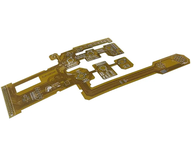
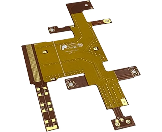
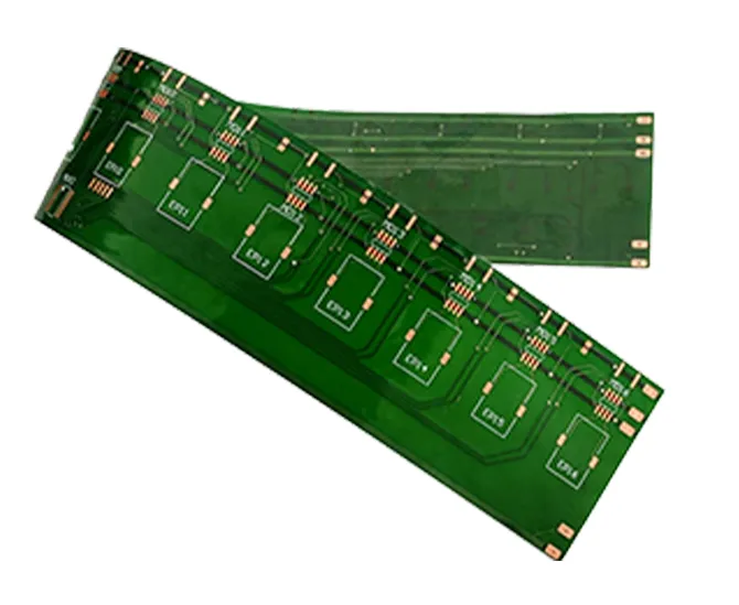
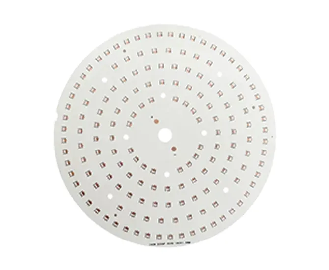
Custom Flexible PCB Boards, from Prototype to Production
A flexible PCB board, also called a flexible printed circuit or FPC, carries conductive copper patterns on a flexible insulating film. It can connect sections of an electronic product while fitting around constrained spaces, reducing the need for separate wires and connectors in suitable designs.
Our flexible PCB fabrication service supports single-sided, double-sided and multilayer constructions. We review the circuit outline, bend areas, copper distribution, connector interfaces and assembly requirements together, so the board is designed for its intended installation and operating conditions.
Typical Specifications of 365PCB's Flexible PCB Boards
Use these options to prepare your fabrication requirements. The final stackup, achievable features and acceptance criteria are confirmed during engineering review.
| Specification | Options and project requirements |
|---|
| Base material | Polyimide (PI); discuss PET or specialty laminates where your electrical, thermal or mechanical requirements call for a different material. |
|---|
| Base film thickness | 12–125 µm options, selected with the copper and coverlay structure. Base film thickness is not the finished flexible PCB thickness. |
|---|
| Layer configuration | Single-sided, double-sided and multilayer flex; 1–8-layer constructions, with higher layer counts reviewed on request. Integrated rigid sections are covered by our rigid-flex PCB manufacturing service. |
|---|
| Copper thickness | 0.5–2 oz options. Specify the required copper construction and identify dynamic flex areas when requesting rolled annealed copper. |
|---|
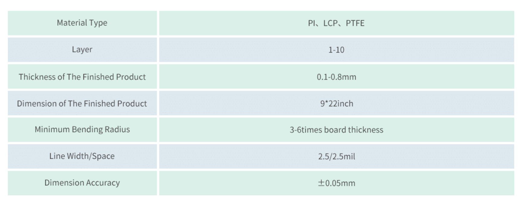
| Finished thickness | 0.1–0.8 mm, depending on construction. The approved stackup defines the finished flexible section; specify local stiffener thickness separately at connector and component areas. Special thickness requirements need engineering review. |
|---|
| Trace width and spacing | Down to 2.5 mil / 2.5 mil (approximately 64 µm / 64 µm), subject to copper thickness and layer construction Submit finer-line requirements for a project-specific review. |
|---|
| Surface finish | ENIG, immersion tin, OSP and hard gold according to pad function and assembly requirements. Selective carbon ink can be reviewed as a separate printed feature. |
|---|
| Coverlay and reinforcement | Coverlay; polyimide, FR-4 or stainless steel stiffeners; pressure-sensitive adhesive where specified. |
|---|
| Additional features | EMI shielding, controlled impedance, blind/buried vias and laser profiling, subject to the complete construction and process review. |
|---|
| Performance requirements | IPC-6013 Class 2 or Class 3 requirements can be specified for review. Agree the applicable revision, product class and inspection requirements before order release. |
|---|
Minimum features and material options are not automatically available in every combination. Your approved fabrication drawing and stackup define the order requirements.
We manufacture to IPC-6013 Class 2/3 standards with the following capabilities:
Base Materials: High-performance polyimide (PI) or polyester (PET), thickness 12–125 µm
Layer Count: 1–8+ layers, including multilayer flex and rigid-flex constructions
Minimum Trace/Space: 50 µm / 50 µm (fine-line capability)
Copper Thickness: 0.5 oz to 2 oz (rolled annealed copper recommended for dynamic flex areas)
Surface Finishes: ENIG, Immersion Tin, OSP, Selective Carbon Ink, Hard Gold
Additional Options: Coverlay, polyimide/FR4/stainless steel stiffeners, EMI shielding, impedance control, blind/buried vias, PSA adhesive, laser profiling
Design Tip: For dynamic flex zones, maintain a bend radius of at least 20× the total board thickness. In static applications, 6–10× is often sufficient. We provide free DFM review to optimize your design for yield and reliability.
Choose Flexible PCB Materials Around the Application
Flexible PCB materials influence bend performance, dimensional stability, assembly compatibility and cost. Polyimide is a common starting point for flexible circuits; the complete laminate system, copper foil, adhesive and coverlay matter as much as the base film.
Polyimide and laminatesDefine the operating environment, soldering process and dimensional requirements. Ask about PET, LCP or PTFE constructions if your application requires an alternative.
Copper selectionReview copper thickness and foil type against current requirements and the intended bend duty. More copper can also increase stiffness in the flex area.
Coverlay and stiffenersProtect conductors while keeping pads accessible. Add local support for connectors and assembly without making the intended bend zone unnecessarily rigid.
For material-specific requirements, see our polyimide PCB capabilities.
Why Choose Our Flexible PCBs?
Ultra-Light & Ultra-Thin Profile — Boards as thin as 0.05 mm and up to 70% lighter than traditional rigid PCBs, perfect for portable, wearable, and space-constrained devices.
High-Density Circuitry — Minimum trace width/spacing down to 50 µm / 50 µm, enabling complex designs without increasing footprint or adding connectors.
Dynamic & Static Flexibility — Engineered to withstand repeated bending, folding, and 3D shaping. Ideal for moving parts, sliding mechanisms, or foldable products.
Proven Durability — Excellent resistance to vibration, shock, and extreme temperatures (-40°C to +150°C+). Fewer solder joints mean higher long-term reliability.
Superior Thermal Performance — Polyimide base material provides efficient heat dissipation, critical for high-power or dense components.
Excellent Solderability & Assembly Compatibility — Multiple surface finishes ensure strong, defect-free SMT assembly and long-term stability.
Compared to rigid PCBs and traditional wiring, flexible circuits can reduce overall assembly weight by over 60%, eliminate bulky connectors, and dramatically improve signal integrity in compact layouts
Flexible PCB vs Rigid PCB Comparison Table
| Feature | Traditional Rigid PCB | Our Flexible PCB (FPC) | Key Benefit |
| Flexibility | None | Static or dynamic bending/folding | True 3D design freedom |
| Weight & Thickness | Heavier and thicker | Up to 70% lighter, as thin as 0.05 mm | Ideal for wearables & portables |
| Space Utilization | 2D flat layout | 3D conformal shaping | Smaller product size |
| Vibration & Shock Resistance | Moderate | Excellent (fewer interconnects) | Automotive & aerospace grade |
| Signal Integrity | More connectors = potential loss | Shorter paths, better performance | High-speed applications |
| Reliability in Dynamic Use | Poor | Designed for millions of flex cycles | Foldable devices & robotics |
| Typical Applications | Fixed equipment | Wearables, medical, EVs, drones | - |
Competence of Flexible PCB
Common Flexible PCB Applications
Choose a flexible circuit around the interconnect, packaging and operating requirements of the device. The examples below show where flex can be useful; the final construction is application-specific.
| Consumer electronics | Wearables and medical devices |
| Display, camera and internal interconnects in smartphones, tablets and other compact devices. Priorities include fitting the enclosure and maintaining reliable contacts. | Compact sensor connections, wearable monitors and portable diagnostic equipment. Define motion, cleaning exposure and the product’s validation requirements. |
| Consumer electronics PCB options | Medical device PCB requirements |
| Automotive and EV electronics | Industrial and robotics |
| Camera, display, lighting and battery-monitoring interconnects. Review installation strain, temperature exposure, vibration and traceability requirements. | Moving sensor links and compact machine connections. Repeated movement needs a specified bend path and representative life testing. |
| Automotive PCB manufacturing | Industrial control PCB options |
| Drones and aerospace electronics | IoT and connected devices |
| Space-conscious interconnects in lightweight electronic assemblies. Specify the operating environment and qualification scope before selecting the construction. | Flexible sensor connections and compact modules. Coordinate antenna clearance, shielding and signal requirements with the physical layout. |
| Aerospace PCB project requirements | IoT and edge-device assembly |

Our Flexible PCB Fabrication Process
The flexible PCB manufacturing process follows the approved construction. Layer count, plated holes, surface finish and reinforcement determine the detailed production route.
01Engineering and file review
Review Gerber and drill files, outline, stackup, bend areas and acceptance requirements. Resolve manufacturability questions before releasing production data.
02Material preparation and circuit patterning
Prepare the selected laminate and form the copper circuitry. Flexible PCB printing requirements should identify the conductor system: copper circuitry and circuits made with conductive inks use different materials and fabrication methods.
03Interconnect formation
Produce holes, plating and layer connections where required by the design. Single-sided and multilayer constructions use different process routes.
04Coverlay and reinforcement
Apply the specified coverlay, laminate the construction and add stiffeners or adhesive features in the defined locations.
05Finish, profiling and inspection
Apply the selected pad finish, complete the outline and inspect the board against approved dimensional and electrical requirements.
06Delivery or assembly
Supply bare flexible boards or continue with component placement, soldering and the agreed assembly tests.
Combine fabrication with flex and rigid-flex PCB assembly when your project needs populated boards. For sourcing and broader integration, explore our PCB assembly services.
Partner with Our Flexible PCB Experts
From initial design consultation to volume production, we provide end-to-end support—including rapid prototyping, strict quality control, and seamless integration with your assembly process. Our focus on PCB design for manufacturing ensures that every flexible circuit is optimized for reliable fabrication, from material selection to fine-line tolerances.
To deliver fully assembled boards ready for deployment, we combine fabrication with expert PCB assembly services—handling component placement, soldering, and testing under one roof.
Our Manufacturing Strengths
One-Stop Solution — From design consultation and DFM optimization to quick-turn prototyping (as fast as 48–72 hours), volume production, component sourcing, SMT assembly, and functional testing — all under one roof.
Strict Quality Control — ISO 9001, IATF 16949, UL certifications. 100% electrical testing, AOI, X-ray, and flex-cycle endurance verification.
Expert Team — Over a decade of specialized experience in high-density flex and rigid-flex boards.
Customer-First Approach — Competitive pricing, flexible MOQs, and dedicated engineering support whether you need 10 prototypes or 100,000+ units.
 English