01 — DFX Begins Before Gerber Release
Don't Wait Until the Factory Finds the Problem
The best time to solve a manufacturing problem is: Before It Becomes a Manufacturing Problem.
02 — Design Creates the Production Difficulty
Factory can optimize: stencil, placement, reflow, inspection.
But if the design requires: Impossible access or Extremely narrow manufacturing margin,
process optimization alone cannot completely repair the architecture.
03 — Manufacturing Is Constrained by Design
Design decides: Layer Count, Via Type, Component Pitch, PCB Thickness, Component Spacing, Test Access, Mechanical Access, Assembly Sequence, Material.
The Factory Inherits Those Decisions.
04 — The Real Question
Not: Can somebody fabricate this board?
Ask: Can the Intended Manufacturing Process Build It Repeatedly With Sufficient Margin?
05 — One Successful Board Proves Very Little
Supplier builds: 1 / 1. Great.
What happens at: 100? 1,000? 100,000?
Production Engineering Is About Repeatability.
06 — Manufacturability ≠ Capability Limit
A supplier may technically advertise: Minimum feature X.
But designing every feature at: X
can create an unnecessarily fragile production process.
07 — Capability vs Process Margin
There is a major difference between: Possible and Robust.
08 — Engineering at the Absolute Minimum
If every line, space, via and registration feature sits at the process edge:
small variation becomes: Yield Loss.
09 — Use Technology Where It Creates Product Value
HDI is valuable when architecture requires it.
Microvia is valuable when density requires it.
Fine pitch is valuable when packaging requires it.
But: Advanced Process Should Solve a Product Problem — Not Create One for No Reason.
10 — DFX
IPC-2231A formalizes DFX as a multidisciplinary design-review methodology spanning fabrication/manufacturing, assembly, testability, cost, reliability, environment and reuse.
For365PCB, we can expand this thinking into: DFM + DFA + DFT + DFR + DFS + DFC + DFSC
11 — DFM
Design for Manufacturing Can the Parts Be Fabricated Repeatedly?
12 — DFA
Design for Assembly Can the Product Be Assembled Correctly, Efficiently and Repeatedly?
13 — DFT
Design for Testability Can Manufacturing Detect the Failures That Matter?
14 — DFR
Design for Reliability Will Expected Variation, Stress and Use Still Leave Enough Margin?
15 — DFS
Design for Serviceability Can the Product Be Diagnosed and Serviced Without Unnecessary Complexity?
16 — DFC
Design for Cost Does the Architecture Achieve Cost Efficiently Without Removing Reliability Margin?
17 — DFSC
Design for Supply Chain Can the Product Continue to Be Built When Components, suppliers and lifecycle conditions change?
18 — These Are Not Separate Problems
A component relocation may:
improve: Assembly.
but worsen: RF.
Changing the PCB stack-up may:
reduce: Cost.
but worsen: SI.
Removing test points may:
increase: Routing space.
but reduce: Test coverage.
DFX Is Multi-Objective Engineering.
19 — Optimize the Product — Not the Discipline
This is one of the best overall365PCB philosophies: Optimize the Product — Not the Discipline.
20 — Start With the Intended Production Model
Ask: Prototype only? Low volume? Medium volume? High volume?
Because: The Optimal Design Changes With Volume.
21 — Prototype Manufacturing
Prototype can tolerate:
more manual work
more rework
slower test.
22 — Volume Manufacturing
At scale: One Extra Minute × 100,000 Units
becomes: 100,000 Extra Minutes.
23 — Assembly Seconds Become Business Economics
A screw.
A connector.
A calibration step.
A manual check.
Every operation has: Time.
24 — DFX Begins With the Manufacturing Flow
Conceptually: PCB Fabrication → Incoming Material → Solder Paste → Placement → Reflow → Inspection → Through-Hole / Secondary Assembly → Programming → Electrical Test → Mechanical Assembly → Calibration → Final Functional Test
Design Should Support the Intended Flow.
25 — PCB Fabrication DFM
First question: Can the Bare PCB Be Manufactured Robustly?
26 — Stack-Up
Stack-up affects:
thickness
impedance
routing
lamination
cost.
Stack-Up Is Manufacturing Architecture.
27 — Standard Material Availability
A technically attractive dielectric may introduce:
sourcing
lead-time
qualification
complexity.
Material Selection Is Supply-Chain DFM.
28 — Layer Count
Fewer layers may reduce: Board Price.
But can increase:
routing congestion
return-path problems
EMI risk.
Cheapest Layer Count Is Not Always Lowest Product Cost.
29 — Layer Count vs Yield
Adding one pair of layers may simplify:
routing
reference planes
assembly risk.
Cost Optimization Should Include Yield Risk.
30 — Board Thickness
Thickness influences:
Mechanical
Via Aspect Ratio
Connector
Impedance
Cost
Board Thickness Is Cross-Functional.
31 — Copper Thickness
Copper influences:
current
impedance geometry
etching behavior.
Electrical Requirement Becomes Fabrication Requirement.
32 — Fine Lines
Very narrow conductors can increase: Process Sensitivity.
Use them where density requires them.
33 — Fine Space
Similarly: Every Micron of Spacing Margin Can Become Manufacturing Margin.
34 — Etch Compensation
Fabricated copper geometry does not always equal: Artwork Geometry.
Manufacturing processes transform geometry.
35 — Controlled Impedance
DFM should coordinate:
Material
Dielectric Thickness
Copper
Trace Geometry
Fabrication Tolerance
Impedance Is a Manufactured Characteristic.
36 — Nominal 50 Ω Is Not the Whole Requirement
The important question is: What Distribution Will Production Produce?
37 — Stack-Up Before Layout
Do not completely route a high-speed PCB and then ask supplier: What stack-up can you make? Layout Should Begin From a Manufacturable Stack-Up.
38 — IPC-2221C Context
Current IPC-2221C remains the generic board-design baseline, while more specialized sectional standards cover rigid, flex and RF board categories.
Use the Applicable Design Framework — Not One Generic Rule for Every PCB.
39 — Drill Architecture
Every drill creates: fabrication, plating, registration.
requirements.
Hole Architecture Is Manufacturing Architecture.
40 — Through Via
Mature.
Cost-effective.
But consumes all relevant layers.
41 — Blind Via
Can improve: routing density.
But adds: fabrication complexity.
42 — Buried Via
Can free external routing.
Again: More Interconnect Complexity Requires More Process Control.
43 — Microvia
Microvia can enable: fine-pitch BGA, HDI.
But: Use It as a System Architecture Choice.
44 — Stacked Microvia
Stacking introduces greater process complexity than some alternative structures.
Density Must Justify Risk.
45 — Staggered Microvia
Can offer different manufacturability trade-offs.
Interconnect Architecture Should Be Selected With the Fabricator.
46 — Via-in-Pad
Excellent for: dense BGA, thermal pad
when implemented with the appropriate process.
But: Via-in-Pad Is a Fabrication + Assembly Decision.
47 — Open Via in Solder Pad
Can affect: solder volume.
Fabrication Geometry Can Become Assembly Defect.
48 — Aspect Ratio
Hole geometry relative to board thickness influences plating-process difficulty.
Don't Treat a Via as Only a CAD Hole.
49 — Annular Ring
Registration variation matters.
Nominal Alignment Is Not Manufactured Alignment.
50 — Drill-to-Copper Clearance
Small margins can turn: Layer Registration Variation
into: Defects.
51 — Backdrill
Backdrilling may improve high-speed channel performance.
But requires:
SI Feature Becomes Fabrication Process.
52 — Controlled Depth
The designer must consider: Manufacturing Tolerance
when defining residual stub targets.
53 — Mechanical Drill vs Laser Process
Different via technologies create different:
trade spaces.
Select Interconnect Technology Intentionally.
54 — Panel Utilization
Board dimensions influence: How Many Units Fit on a Manufacturing Panel.
55 — One Millimeter Can Change Panel Economics
A small board-outline change can sometimes improve: Panel Utilization.
That can reduce cost without touching electronics.
56 — But Don't Distort the Product for Panelization Alone
Again: Optimize Total Product.
57 — Panel Rails
Assembly may require:
outside the final PCB.
Manufacturing Needs Temporary Geometry Too.
58 — Breakaway Strategy
Tabs / routed edges / scoring approaches affect:
board edge
component clearance
depanelization stress.
Panelization Should Be Considered During PCB Layout.
59 — Edge Components
Components too close to a break region can experience: Mechanical Risk.
60 — Connector at Board Edge
May influence:
Final Product Geometry and Manufacturing Geometry Interact.
61 — Fiducials
Machine vision needs reliable positional references.
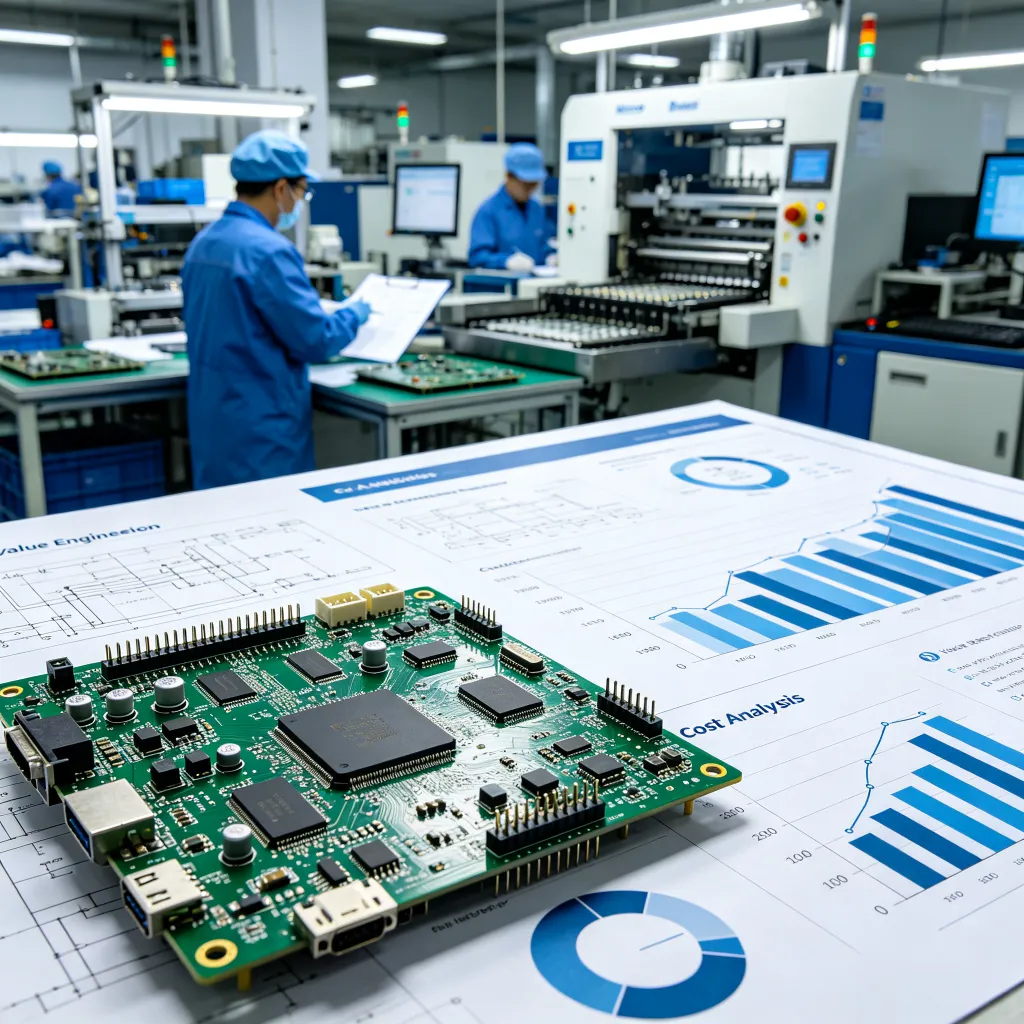
Placement Accuracy Begins With Registration.
62 — Global / Local Registration Inputs
Dense/fine-pitch layouts may benefit from appropriate machine-vision references according to assembly process.
Equipment Must Know Where the Board Actually Is.
63 — PCB Surface Finish
Surface finish can influence:
solderability
planarity
contact
RF
according to application.
Finish Is a Functional Material Choice.
64 — Finish Availability
A finish that only one specialist supplier supports creates: Supply-Chain Risk.
65 — Solder Mask
Mask geometry affects:
soldering
bridging
exposed copper.
Solder Mask Is Assembly Geometry.
66 — Mask Registration
Actual manufacturing introduces: Registration Variation.
67 — Solder Mask Defined vs Non-Solder-Mask Defined
Choice can affect:
pad geometry
reliability
assembly.
Pad Architecture Should Follow Package and process requirements.
68 — Land Pattern
One of the most important DFA/DFM interfaces.
Component Footprint Is Where Component and Manufacturing Process Meet.
69 — Don't Blindly Copy Datasheet Footprints
Vendor footprint may optimize:
one evaluation board
one process.
Product Land Pattern Needs Manufacturing Context.
70 — IPC Land Pattern Status
IPC currently marks legacy IPC-7351 as no longer maintained and lists IPC-7352, released in 2023, as the newer generic land-pattern guideline.
This is exactly the kind of standards-status detail365PCB should get right.
71 — Component Tolerance
Land pattern must account for: Component Dimensional Variation, Board Fabrication Variation, Placement Variation.
Footprint Is a Tolerance Problem.
72 — Courtyard
A component's needed space is larger than: Its Plastic Body.
73 — Placement Courtyard
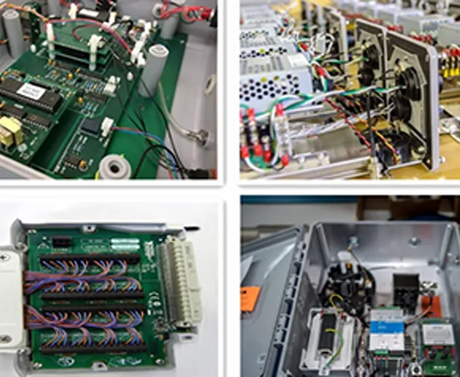
Need room for:
adjacent components
assembly
inspection
rework.
Density Has a Service Cost.
74 — Ultra-Dense Placement
Very tight placement may reduce PCB area.
But increase:
rework difficulty
inspection difficulty
thermal coupling.
Smaller Is Not Automatically Better.
75 — Component Orientation
Consistent orientation can simplify:
assembly
inspection
visual review.
Orientation Can Reduce Human Error.
76 — Polarity
Polarity markings should be: clear, unambiguous.
Prevent Wrong Assembly by Design.
77 — Reference Designators
Readable identification supports: debug, rework, service.
Silkscreen Can Be Engineering Infrastructure.
78 — Silkscreen ≠ Decoration
It can communicate: orientation, connector, test point, information.
79 — BGA
BGA combines:
PCB Fabrication
Assembly
X-Ray
Routing
Reliability
BGA DFM Is Multi-Discipline.
80 — BGA Pitch
Pitch determines: land pattern, escape, via technology.
Package Selection Can Define PCB Technology.
81 — BGA Escape
If a selected processor forces: HDI, multiple laminations.
that is not simply: Layout Detail.
It can become: Product Cost Architecture.
82 — Package Before PCB
Component selection and PCB manufacturing capability should communicate early.
Silicon Package Can Determine Factory Process.
83 — IPC-7095E
IPC's revision table lists IPC-7095E, released in 2024, for BGA design and assembly process implementation.
Advanced Packages Deserve Package-Specific Engineering.
84 — BGA X-Ray Access
Can the hidden interconnect be meaningfully inspected?
Inspection Strategy Begins at Design.
85 — Under-BGA Test Access
Dense BGA escape can consume: Test-Point Opportunity.
So DFM and DFT must work together.
86 — QFN / BTC
Bottom-terminated packages create: thermal pad, solder-volume, hidden-joint, considerations.
Package Footprint Is Process Design.
87 — Thermal Pad Paste
Too much or too little solder can influence: standoff, voiding, thermal contact, depending on package/process.
Stencil Design Is Product Engineering.
88 — Stencil
Stencil apertures control: Solder-Paste Deposition.
89 — IPC-7525C
Current IPC revision information lists IPC-7525C for stencil-design guidelines.
Paste Volume Should Be Designed — Not Discovered After Defects Appear.
90 — Paste Printing
Manufacturing begins with: Depositing the Correct Volume in the Correct Location.
91 — Very Small Components
Small packages require more demanding: paste, placement, process, control.
Package Miniaturization Narrows the Process Window.
92 — Large + Small Components Together
A board with: Large Connector, Tiny Passives, Large BGA.
can be much more difficult than one containing only one package family.
Mixed Technology Creates Process Compromise.
93 — Thermal Mass
Heavy components heat differently during soldering.
PCB Assembly Is a Thermal System.
94 — Reflow Profile
Current IPC-7530B, released January 2025, is the IPC guideline for temperature profiling in mass soldering processes.
Reflow Is Not "Put the Board in an Oven."
95 — Component Mix
Board: copper, component mass, layer count, changes thermal behavior.
The Same Oven Recipe Is Not Automatically the Same Process.
96 — DFM Should Ask About Reflow Before Production
Can the design achieve an acceptable thermal process window across: All Critical Components?
97 — Heat-Sensitive Components
Some components have particular processing constraints.
Component Selection Can Affect Assembly Process.
98 — MSL
Moisture sensitivity and handling requirements can affect: storage, preparation, production flow.
Component Package Has a Factory Lifecycle.
99 — High-Value Components
More expensive devices increase the financial consequence of: Process Failure.
100 — DFA
Now we shift from: Can we fabricate it?
to: Can we assemble it well?
101 — Assembly Sequence
A final product has an order: PCB → Harness → Thermal Hardware → Enclosure → Final Test.
Design the Sequence Before Writing the Work Instruction.
102 — Part Count
Each additional part adds: sourcing, handling, assembly, opportunity.
Every Part Should Have a Functional Reason.
103 — Fastener Count
Reducing unnecessary fasteners can improve: assembly time, error rate, service.
104 — Fastener Variety
Ten different screw types may create: Operator Confusion.
105 — Standardization
Use common:
fasteners
connector families
where product architecture allows.
Standardization Is DFA + Supply-Chain Engineering.
106 — Orientation
A part installable: Four Ways
but correct in only: One Way
is an assembly risk.
107 — Keying
Mechanical or electrical keying can make incorrect installation: Impossible or More Difficult.
108 — Poka-Yoke
Design error-proofing into: Geometry.
Prevention Is Better Than Operator Training Alone.
109 — Connector Keying
Similar connectors near each other can create: Assembly Mistakes.
110 — Harness Labels
Clear identity can improve: assembly
service.
Harness Is Part of DFA.
111 — Cable Length
Too short: difficult assembly.
Too long: routing, airflow, cost.
Harness Geometry Is Manufacturing Geometry.
112 — Cable Bend
Assembly should not require: Uncontrolled Force.
113 — Tool Access
A screw may exist in CAD.
But: Can the Production Tool Reach It?
114 — Driver Angle
If operators must hold the driver at a difficult angle: Torque Consistency May Suffer.
115 — Torque
Fasteners affecting:
may require controlled assembly.
Mechanical Assembly Can Control Electrical/Thermal Performance.
116 — Hidden Fastener
If screw cannot be inspected: How Do We Verify It Was Installed?
117 — Captive Fastener
Can reduce: lost hardware
service error.
118 — Adhesive
Adhesive introduces:
inspection.
Adhesive Is an Assembly Process.
119 — Cure Time
Long cure can become: Production Bottleneck.
120 — Manual Process
Any manual task should prompt: Can this be simplified?
Manual Work Is Not Bad — Uncontrolled Manual Work Is Risky.
121 — Human Variation
Different operators: pressure, speed, technique.
DFA Reduces Dependency on Individual Skill.
122 — Assembly Ergonomics
Repeated difficult motion can reduce: speed, consistency.
Factory Human Factors Are Product Engineering.
123 — Robotic / Automated Assembly
If production may become automated: component access, gripping, alignment, can influence architecture.
Design Can Enable Automation.
124 — But Don't Automate a Poor Design
First: Simplify the Assembly.
Then automate when economics justify it.
125 — Mixed SMT / Through-Hole
Some components may require: secondary processes.
Every Extra Process Stage Adds Handling.
126 — Through-Hole Placement
Consider: accessibility, solder process, mechanical stability.
127 — Selective Solder / Wave Inputs
Package location and bottom-side components can influence process feasibility.
PCB Layout Should Understand the Assembly Method.
128 — Hand Solder as Production Strategy
Acceptable in some low-volume/specialized contexts.
But if high volume requires thousands of manual joints: Revisit Architecture.
129 — Reworkability
No production process is perfect.
Ask: Can Defects Be Reworked Without Destroying Nearby Components?
130 — BGA Rework Clearance
Components positioned too close to BGA can obstruct: rework tools.
Dense Layout Can Increase Repair Cost.
131 — Rework vs Reliability
Rework can restore product.
But excessive rework signals: Process Instability.
132 — IPC-7711/21D
IPC lists IPC-7711/21D, released in 2024, as the current rework/modification/repair document.
Rework Should Be Controlled — Not a Substitute for Good DFA.
133 — Inspection Accessibility
Can: AOI, see the joint?
Can: X-Ray, interpret the hidden structure?
Can: Operator, verify orientation?
Inspection Is Designed Too.
134 — AOI Shadowing
Tall components can obstruct: Camera View.
135 — Reflective / Hidden Geometry
Some joints are harder to inspect optically.
Test Strategy Should Follow Defect Visibility.
136 — Process vs Acceptance
Current IPC standards make an important distinction: J-STD-001J defines assembly process/material requirements, while IPC-A-610J is a post-assembly acceptance standard.
A Product Can Look Acceptable Without Proving the Process Was Robust.
137 — Final Inspection Is Not DFM
If the process creates defects and inspectors remove them: Quality Was Detected — Not Built In.
138 — Design for Process Stability
A better architecture makes: Correct Assembly the Normal Outcome.
139 — DFT
Now comes one of the most underestimated areas: Design for Testability.
140 — Testing Is Not Added at the End
When layout is finished:
there may be: No Physical Access Left.
141 — DFT Starts During Architecture
Ask: What failures must production detect? At what stage? Through what interface?
Test Strategy Should Exist Before PCB Freeze.
142 — Test Coverage
Test coverage asks: Which Potential Failures Can the Manufacturing Test Actually Detect?
143 — 100% Functional Coverage Is Not the Same as 100% Defect Coverage
A product boots successfully.
Can it still contain: wrong component value? marginal solder joint? unused broken interface?
Functional Test Sees Behavior — Not Every Physical Defect.
144 — Different Tests See Different Failures
SPI
Solder paste deposition.
AOI
Visible assembly conditions.
X-Ray
Selected hidden structures.
ICT
Electrical component/net access.
FCT
Product behavior.
Boundary Scan
Selected digital structural interconnects.
No One Test Sees Everything.
145 — Layered Test Strategy
A strong test architecture can use: Several Complementary Detection Layers.
146 — Test Earlier Where Possible
Defect detected immediately after: Paste Printing
is cheaper than detecting it after: Full Box Build.
147 — Cost of Detection Rises Downstream
PCB Fabrication → SMT → Box Build → Customer
The Later the Defect Is Found, the More It Often Costs.
148 — Test Point
A test point looks small.
But it provides: Physical Access to Electrical State.
149 — Test Access Is a Board Resource
Test point consumes: area, routing, spacing.
DFT Competes for PCB Real Estate.
150 — Reserve Access Early
Don't finish routing and ask: Where can we squeeze 200 test points? Allocate Testability During Placement and Routing.
151 — Power-Rail Access
Production may need access to: important rails.
Power Testability Should Be Designed.
152 — Ground Access
Probe systems need appropriate: Reference Connections.
153 — Programming Access
MCU / FPGA / memory may require: programming, verification.
Programming Is a Manufacturing Process.
154 — Programming Connector
Development connector may be too: large, costly, for production.
Development DFT and Production DFT May Differ.
155 — Pogo Pads
Dedicated test pads can support fixture contact.
Temporary Interface Can Reduce Production BOM.
156 — Fixture Access
Mechanical housing, heatsink or connector can block: Test Fixture.
157 — Test Stage Selection
Maybe PCBA should be tested: Before Housing Assembly.
Then final system only receives: Short Final Test.
158 — Separate Board Test and System Test
This can improve: fault localization.
Know Which Assembly Stage Introduced the Failure.
159 — ICT
In-circuit testing can identify selected: opens, shorts, component characteristics, where access/design support it.
ICT Effectiveness Is Designed Into the PCB.
160 — Flying Probe
Can provide flexible test access for: prototypes, lower-volume bare-board/assembly strategies, depending on process.
Test Economics Change With Volume.
161 — Bed-of-Nails Fixture
High volume may justify dedicated fixture investment.
Volume Changes Test Architecture.
162 — Fixture Cost vs Cycle Time
Dedicated fixture: higher upfront cost, potentially faster execution.
Manufacturing Economics Should Be Modeled.
163 — Boundary Scan
JTAG/boundary-scan-capable devices may support structural testing of selected digital interconnects.
Silicon Can Participate in Manufacturing Test.
164 — But Boundary Scan Must Be Architected
Need: chain, access, compatible devices.
DFT Is Hardware Architecture.
165 — BIST
Built-In Self-Test can allow the product to test: Itself.
166 — Memory Test
Firmware can test: RAM, Flash, under defined production procedures.
Software Can Be a Manufacturing Instrument.
167 — Peripheral Self-Test
Selected: sensors interfaces, may have diagnostic capabilities.
Use Product Intelligence to Improve Test Coverage.
168 — Loopback
Communication interfaces may support: Controlled Loopback to isolate faults.
169 — FCT
Functional Test asks: Does the Product Behave Correctly?
170 — Production FCT Is Not DVT
DVT may take: Hours.
Production FCT may need: Seconds or Minutes.
Qualification and Production Test Have Different Objectives.
171 — DVT Proves the Design
Production Test controls: Manufacturing Escape Risk.
172 — Test Compression
The engineering challenge: Detect the Important Failures in the Minimum Responsible Time.
173 — Test Time Is Cost
10 seconds × 1 million units: Significant Factory Capacity.
174 — But Removing Test Can Cost More
If field failures increase: Saved Seconds Become Expensive Returns.
175 — Test Optimization
Balance:
Coverage
Cycle Time
Fixture Cost
Diagnosis
Escape Risk
DFT Is an Optimization Problem.
176 — Test Parallelization
Where architecture allows: several measurements/functions can execute concurrently.
Design Can Reduce Test Time.
177 — Device Boot Time
A device needing: 3 minutes to boot
creates production-test implications.
178 — Factory Boot Mode
Product can have a controlled manufacturing-test mode.
Manufacturing Software Is Part of DFT.
179 — But Factory Mode Needs Security Architecture
A privileged factory mode should not accidentally remain: An Uncontrolled Customer Backdoor.
This connects Page 34.
180 — Test Firmware
Dedicated test firmware can make: hardware validation, manufacturing diagnostics, more efficient.
Firmware Can Increase Test Observability.
181 — Product Firmware vs Test Firmware
Need version/configuration control.
Software Configuration Is Manufacturing Configuration.
182 — Programming Verification
Do not only: Send the File.
Verify appropriate evidence that: Intended Image Reached the Intended Unit.
183 — Device Identity
Serial number / firmware / calibration can be associated.
Testability Can Support Traceability.
184 — Calibration
Some products require per-unit calibration.
Calibration Is Not the Same as Test.
185 — Calibration Adjusts
Test determines: Whether Requirement Is Met.
Calibration changes: Product Parameters to improve alignment.
186 — Calibration Time
If calibration takes: 20 minutes per unit, it may dominate production economics.
187 — Design for Calibration
Can the product automatically: acquire references, calculate coefficients
where appropriate? Product Architecture Can Reduce Factory Time.
188 — Calibration Storage
Coefficients need: integrity, unit association.
Calibration Is Product Configuration.
189 — Calibration Access
Need a path to: Enter / Verify, calibration data.
190 — Testability and Root Cause
A failed FCT that only reports: FAIL
is much less useful than: Rail 3V3 outside defined limit.
Good DFT Improves Diagnosis.
191 — Fault Localization
Ask: Can Test Tell Us Where to Look?
192 — Diagnostic Resolution
More diagnostics can reduce: technician time scrap.
Test Architecture Affects Repair Economics.
193 — No-Fault-Found
Products that fail once but cannot be reproduced consume enormous resources.
Observability Reduces NFF.
194 — DFR
Manufacturing robustness is not only: Yield Today.
It must support: Reliability Tomorrow.
195 — Component Derating
Design should avoid relying unnecessarily on: Absolute Limits.
196 — Electrical Margin
Production variation can consume:
margin.
Reliability Begins With Margin.
197 — Mechanical Margin
Connector alignment should tolerate: Real Part Distribution.
198 — Thermal Margin
TIM thickness variation should not immediately create: Overtemperature.
199 — RF Margin
Antenna should tolerate expected:
variation.
200 — SI Margin
Impedance / via / material variation should remain within: Channel Budget.
201 — Robust Design
The goal is not: Perfect Nominal Unit.
The goal is: Acceptable Population.
202 — Monte Carlo / Corner Analysis
Where appropriate: simulate component and manufacturing variation.
Design for the Distribution.
203 — Worst-Case Circuit Analysis
Selected analog/power designs can assess:
tolerance
temperature
aging
corners.
Nominal Simulation Is Only the Center.
204 — Tolerance Stack-Up
Mechanical dimensions accumulate.
Assembly Yield Can Be Predicted Before Tooling.
205 — Process Capability and Design
If specification requires a tolerance much tighter than process can reliably produce:
two options: Improve Process or Change Design.
Sometimes the Best Process Improvement Is a Better Design.
206 — Manufacturing Yield Is Partly Designed
This is a powerful statement: Yield Is Not Only a Factory Metric.
Yield Is Also a Design Outcome.
207 — Design-Induced Yield Loss
Examples:
tiny solder margin
difficult escape
inaccessible test point
weak mechanical datum.
Production Data Can Reveal Design Fragility.
208 — First-Pass Yield
A design requiring constant rework may achieve: Good Final Yield
but still be: Poor DFX.
209 — Rework Is Cost
Every rework adds: labor, delay, additional process exposure.
Design for First-Pass Success.
210 — Design for Supply Chain
A board cannot be manufactured if: Critical Component Cannot Be Purchased.
211 — Sole Source
A unique component can be justified.
But know: Supply Risk.
212 — Alternate Parts
Where business requirements justify it:
design in: Verified Alternatives.
213 — Drop-In Myth
Pin-compatible: ≠ electrically equivalent.
Alternate Must Be Verified.
214 — Package Variation
Alternative device may have: different package, thermal behavior.
Supply-Chain Change Can Become PCB Change.
215 — Lifecycle
Check:
risk during product development.
Product Lifetime Should Influence BOM.
216 — Lead Time
A 52-week component can become: Production Schedule Architecture.
217 — MOQ
Minimum-order economics can affect: Product Cost.
218 — Authorized Sources
Counterfeit risk increases when emergency sourcing becomes necessary.
Good DFSC Reduces Emergency Procurement.
219 — Component Standardization
Reuse common components across product families where appropriate.
Platform Strategy Can Improve Supply Resilience.
220 — Common Passive Values
Unnecessary proliferation can increase: line feeders, inventory.
BOM Complexity Is Manufacturing Complexity.
221 — Unique Part Count
500 line items vs BOM Architecture Affects Factory Complexity.
222 — Design for Cost
Cost engineering should include: More Than Component Price.
223 — Total Product Cost
Consider: PCB, Components, Assembly, Test, Tooling, Yield, Rework, Warranty, Cheapest BOM Can Create Expensive Product.
224 — Remove Unnecessary Complexity
A design may contain: precision part, exotic material, special process, without functional benefit.
Complexity Should Earn Its Cost.
225 — Costed DFM
Ask: What design decision is driving manufacturing cost?
Cost Should Be Traceable to Architecture.
226 — Layer Reduction
Good idea when: SI / PI / EMC / Yield remain acceptable.
227 — HDI Removal
Good idea if architecture allows.
Bad idea if it creates: larger board, impossible escape.
Cost Optimization Is System-Level.
228 — Component Consolidation
One integrated IC can reduce: parts, assembly.
but create: sole-source risk.
Every Optimization Has Trade-Offs.
229 — Connector Reduction
Can reduce:
failure points.
But may reduce: Serviceability.
230 — Design for Serviceability
Some products are disposable.
Others should be serviceable for: Architecture should know which.
231 — Module Replacement
A replaceable: PSU, fan, compute module, can reduce field service cost.
232 — Diagnostic Access
Service technician may need: logs, test interface.
Serviceability Begins in Design.
233 — Don't Hide Every Failure Behind One Error LED
Diagnostic resolution can reduce: Support Cost.
234 — Repair Access
Can a failed part be replaced without: Destroying the Enclosure?
235 — Connector Life
Repeated servicing creates: Mechanical Cycles.
236 — Spare Strategy
Product architecture can influence: Spare-Part Inventory.
237 — Design for Environment
IPC-2231A includes environmental considerations as part of DFX.
This can include: materials, manufacturing, product lifecycle, considerations appropriate to requirements.
238 — Process Chemistry
Manufacturing choices can affect: environmental, regulatory, requirements.
DFX Can Extend Beyond the Product's Electrical Function.
239 — Reuse
Product families may reuse:
fixtures.
Reuse Can Improve Quality When the Reused Design Is Proven.
240 — Reuse ≠ Copy-Paste
The reused design must still fit: New Requirements.
241 — Platform Engineering
A proven: Power Module, Compute Module, Wireless Module, can accelerate later products.
Reuse Validated Architecture — Not Historical Mistakes.
242 — DFX Review Should Be Cross-Functional
Participants can include: Hardware, PCB, Manufacturing, Assembly, Test, Mechanical, Firmware, Quality, Supply Chain.
No Single Engineer Sees Every Production Risk.
243 — DFM Review Before Layout Freeze
Best time to challenge:
stack-up
via technology
package
is: Before Routing Is Locked.
244 — Intermediate DFM Review
Review again after: placement, major routing.
Catch Directional Problems Before Final Release.
245 — Final DFX Review
Before release:
verify agreed issues are: Closed or Accepted.
246 — DFX Issue Register
Each issue should have:
Issue
Risk
Owner
Action
Status
DFX Should Produce Decisions — Not Only Comments.
247 — Severity
Not every DFM violation is equal.
Classify: Critical, High, Medium, Advisory, according to project.
Prioritize Engineering Attention.
248 — "DFM Error" vs "DFM Risk"
Some features violate: Hard Process Capability.
Others are: Possible but Low Margin.
Distinguish them.
249 — Capability Matrix
365PCB should maintain a controlled: Master Capability Matrix.
This is especially important because your website will eventually contain hundreds of technical claims.
250 — Capability Is Process-Specific
Do not say: 0.05 mm always available.
Instead: Capability Depends on Material, layer structure, copper, board thickness and process.
251 — Preferred / Advanced / Review Required
A useful internal model can classify design features: Preferred, Normal robust production.
Advanced
Supported with tighter controls.
Engineering Review Required, Project-specific evaluation.
This Is Much Better Than One "Minimum Capability" Number.
252 — Preferred Design Rules
A preferred rule gives: Production Margin.
253 — Minimum Design Rule
Minimum rule represents: Boundary Capability.
These are not the same.
254 — Customer Education
One of the most valuable roles of365PCB engineering is telling customers: Yes, we might be able to make this.
but: We Recommend Changing It Because We Want Repeat Production to Be Stable.
That is real engineering support.
255 — DFM Should Explain Why
Bad DFM comment: Increase spacing.
Good DFM: Increase spacing because this feature is operating near the selected process-registration margin and could reduce repeat-production yield.
Engineering Feedback Needs Mechanism.
256 — Recommended Change
Provide: Current Condition → Risk → Recommended Change → Expected Benefit
DFM Should Help the Designer Decide.
257 — Customer Constraint
Sometimes change is impossible.
Then: Process Controls Must Compensate.
258 — Risk Acceptance
If customer accepts low margin:
document: The Engineering Decision.
259 — DFM Is Not a Sales Barrier
The objective is not: reject difficult work.
The objective is: Understand the Risk Before Production.
260 — Advanced Designs Sometimes Need Advanced Processes
There is nothing wrong with:
special materials.
Complexity Is Valid When the Product Requires It.
261 — Engineering Support Means Matching Design to Process
Not: Simplifying Every Product.
But: Making Complexity Controlled.
262 — DFT Coverage Planning
A serious DFT review should map: Potential Failure → Detection Method → Test Stage
Every Important Failure Needs a Detection Strategy or an Accepted Risk.
263 — Fault Coverage Matrix
Example:
Failure Mode | SPI | AOI | X-Ray | ICT | FCT |
Missing component | — | ✓ | — | possible | possible |
Hidden BGA issue | — | limited | ✓ | possible | possible |
Firmware function | — | — | — | limited | ✓ |
Actual coverage remains product-specific.
Test Architecture Should Be Explicit.
264 — Don't Overclaim Test Coverage
No system catches: Everything.
The correct question: Which risks are covered, by which method, with what confidence?
265 — Electrical Test Standards Status
One standards caution worth keeping internal: IPC's current revision table marks IPC-9252B, the older requirements document for electrical testing of unpopulated printed boards, as No Longer Maintained.
Therefore365PCB should not casually describe it as the newest/current electrical-test standard. Standards Status Matters.
266 — DFX Data Exchange
Manufacturing should receive: design intent, critical characteristics, test requirements.
Data Quality Is Part of DFM.
267 — Gerber Alone Can Be Incomplete
Complex products often require:
BOM
Pick & Place
Stack-Up
Impedance
Drawings
Test Requirements
Assembly Notes
Manufacturing Needs Product Definition.
268 — Intelligent Manufacturing Data
Structured formats such as IPC-2581 can help transmit richer design/manufacturing data where the workflow supports them.
Data Transfer Can Reduce Interpretation.
269 — Revision Control
DFM should review: The Correct Revision.
270 — BOM / PCB Mismatch
Rev C Gerber + Rev B BOM = Manufacturing Risk.
271 — CAD Library Governance
Wrong footprint creates: Perfectly Manufactured Wrong Product.
272 — Library Qualification
Symbol:
Footprint:
3D:
Pin Mapping: need controlled relationships.
DFM Begins Before Board Layout.
273 — Footprint Error Is Catastrophic Efficiency
Factory may build it: Perfectly.
And every board fails.
Manufacturing Quality Cannot Correct Design Data Error.
274 — Component Manufacturer Changes Package
Same family name may not mean: Same physical geometry.
275 — Incoming DFX Check
Component changes should trigger:
review where relevant.
276 — Supply Chain + DFM Loop
New alternate part: new package → new stencil → new assembly behavior
Purchasing Decisions Can Become Manufacturing Decisions.
277 — DFX and NPI Boundary
This distinction is very important for our page architecture.
Page 39 — DFX
answers: Did We Design the Product to Industrialize Well?
Page 40 — NPI
will answer: How Do We Transfer That Industrialized Design Into a Controlled Production System?
So Page39 focuses on: Design Decisions.
Page40 focuses on: Production Implementation.
278 — DFX Output Should Be Production Inputs
After Page39, engineering should be able to provide Page40 with:
DFX Defines What Production Must Control.
279 — Production Should Feed Back Into DFX
After first builds: Yield Problem → Root Cause → Design Rule Improvement
DFX Is a Learning System.
280 — Factory Feedback Is Design Data
SPI trend.
AOI defect.
X-Ray finding.
ICT failure.
FCT failure.
Manufacturing Data Should Return to Engineering.
281 — Design Rule Improvement
Example: Repeated solder issue on footprint.
Don't only: Tune the Line Forever.
Ask: Can the Footprint Be Improved?
282 — Process Improvement vs Design Improvement
Sometimes: Fix the Process.
Sometimes: Fix the Design.
The best engineering organization knows the difference.
283 — Failure Cost Curve
A design issue found during: CAD review is cheap.
Found during: PVT is expensive.
Found after: Shipment is much more expensive.
DFX Moves Discovery Upstream.
284 — Front-Load Engineering
Spend more engineering effort before production to reduce: Downstream Correction.
285 — This Is Especially Important for High-Value Electronics
When PCB contains:
processor
FPGA
expensive RF devices
a manufacturing escape can cost: Far More Than the PCB.
This directly supports365PCB's positioning: When Failure Costs More Than the PCB.
286 — Complex BOM + DFX
High-value components deserve:
robust footprint
assembly
inspection
test
planning.
Protect the Value Through Design.
287 — DFX for High-Speed Systems
High-speed design must account for: Electrical Performance, Fabrication Tolerance, Assembly.
The CAD Geometry Is Only Nominal.
288 — SI-Aware DFM
Ask: What manufactured geometry distribution will the channel see?
Signal Integrity Can Be a Manufacturing Characteristic.
289 — PI-Aware DFM
Copper/current paths should remain manufacturable while supporting:
requirements.
290 — RF-Aware DFM
RF material and geometry tolerances can affect: Frequency Performance.
291 — Thermal-Aware DFM
Thermal vias, pads, TIM interfaces and copper should be: Manufacturable and repeatable.
292 — Mechanical-Aware DFM
Tolerance chain should support:
seal.
Mechanical Yield Is Product Yield.
293 — AI-Aware DFM
Camera / microphone / sensor assembly variation can change: Model Input.
Therefore: AI Accuracy Can Have Manufacturing CTQs.
294 — Cybersecurity-Aware DFT
Production test may verify:
security state.
Cybersecurity Can Become EOL Test Requirement.
295 — OTA-Aware DFM
Hardware needs enough:
Field Maintainability Can Be a PCB Design Requirement.
296 — Design Margin
The central philosophy of Page39 is: Margin.
297 — Electrical Margin
Enough voltage/timing/noise margin.
298 — Mechanical Margin
Enough tolerance/clearance margin.
299 — Thermal Margin
Enough temperature/interface margin.
300 — Manufacturing Margin
Enough process window.
301 — Test Margin
Enough difference between: Good and Bad for test system to distinguish them.
302 — Supply Margin
Enough sourcing flexibility.
303 — Margin Is What Makes Scale Possible
One prototype can survive: Coincidence.
10,000 units require: Margin.
304 — Design for Nominal vs Design for Population
This is one of the strongest concepts: Nominal Design Asks Whether the Ideal Product Works.
DFX Asks Whether the Population Works.
305 — Production Is a Distribution
Components vary.
PCB varies.
Placement varies.
Reflow varies.
Mechanics vary.
Real Products Are Distributions.
306 — Robust Product
A robust design creates a functional distribution that remains: Inside Requirements.
307 — Quality Is Designed Upstream
Inspection can identify: Bad Product.
DFX reduces: How Often Bad Product Is Created.
308 — The Factory Should Not Be Forced to Manufacture Around the Design
The design should help: The Factory Succeed.
309 — The Best DFM Comment May Remove a Process Step
For example:
changing architecture could eliminate: manual jumper, special secondary operation.
Simplification Can Improve Quality and Cost Simultaneously.
310 — The Best DFA Change May Remove an Assembly Error
One keyed connector:
can eliminate: Entire Failure Mode.
311 — The Best DFT Change May Save Hours of Debugging
One strategically placed access point:
may convert: mysterious fail
into: Clear diagnosis.
312 — Design for Detectability
An important high-level idea: If a Critical Failure Cannot Be Prevented Completely, Make It Detectable.
313 — Design for Recoverability
For software-enabled products:
some failures should be: Recoverable.
This links Pages33/34.
314 — Design for Traceability
If a critical issue occurs: Can We Determine Which Units Are Affected?
315 — Serial Identity
Product identity enables:
correlation.
Traceability Is Root-Cause Infrastructure.
316 — DFX and Quality Planning
Critical product characteristics discovered during DFX can later become:
control-plan
inspection
test
inputs.
Design Risk Becomes Manufacturing Control.
317 — CTQ Definition
Examples:
BGA assembly
Impedance
Connector alignment
TIM gap
Firmware version
depending on product.
Control What Controls the Product.
318 — PFMEA Input
Detailed manufacturing PFMEA belongs more strongly in Page40, but Page39 should identify: Design Features That Create Process Risk.
319 — DFMEA Input
Similarly, design risk analysis can identify: Where manufacturing variation could produce product failure.
320 — Critical Characteristic Cascade
Product Requirement → Design Parameter → Manufacturing Characteristic → Measurement
Requirements Can Be Translated Into Factory Controls.
321 — Example: Antenna Performance
Requirement: Wireless performance.
Design parameter: antenna geometry.
Manufacturing characteristic: enclosure material / antenna location.
Measurement: defined RF verification.
DFX Connects Physics to Production.
322 — Example: CPU Temperature
Requirement: junction temperature limit.
Design: TIM / heatsink geometry.
Manufacturing characteristic: interface gap / clamp condition.
Measurement: assembly / functional validation.
323 — Example: High-Speed Link
Requirement: channel margin.
Design: stack-up / via geometry.
Manufacturing characteristic: dielectric / copper / drill.
Measurement: impedance / SI evidence where required.
324 — This Is Advanced DFX
Not: 6 mil spacing passed.
But: Which Manufactured Variable Controls Which Product Requirement?
That is world-class thinking.
325 — DFX Digital Thread
Potential chain: Requirement → Design → DFX Risk → Manufacturing Characteristic → Inspection / Test → Yield → Field Result
Design for Excellence Can Be Traceable.
326 — Prototype Feedback
Page37 produces: Physical Learning.
327 — EVT Feedback
Page38 produces: Architecture Evidence.
328 — DVT Feedback
Produces: Product Evidence.
329 — DFX Converts the Learning Into Production-Robust Design
This is the bridge.
330 — Page40 Will Then Industrialize It
NPI Converts That Design Into a Controlled Factory System.
This creates a very clean architecture between pages39 and40.
331 — What Does World-Class DFM / DFA / DFT Engineering Look Like?
At the highest level: Product Requirements → Manufacturing Strategy → Target Production Volume → PCB Technology Selection → Stack-Up → Materials → Via Architecture → Component Package Selection → Land Pattern → Placement Architecture → Panelization Inputs → Fabrication DFM → Assembly Process Selection → Stencil / Paste Inputs → Reflow / Secondary Process Inputs → DFA → Part Count → Assembly Sequence → Error Proofing → Tool Access → Serviceability → Inspection Accessibility → DFT → Fault Model → Test Coverage → Test Points → Programming → ICT / Boundary Scan / FCT → Calibration → Test Cycle Time → DFR → Tolerance / Margin → Supply-Chain Robustness → Cost Optimization → Cross-Functional DFX Review → DFX Issue Closure → Prototype / EVT Feedback → Manufacturing Risk Reduction → Production-Robust Product Design
That is the difference between: Designing a Product That Can Be Built
and: Designing a Product That Is Ready to Be Built Well.
Typical DFM / DFA / DFT Engineering Deliverables
Depending on project requirements, a 365PCB ODM DFX program may include:
DFX Strategy
Manufacturing Feasibility Review
Product Industrialization Inputs
Target-Volume Review
Manufacturing-Process Selection Inputs
PCB Fabrication DFM
PCB Stack-Up DFM
PCB Material Review
PCB Thickness Review
Layer-Count Optimization Inputs
Controlled-Impedance DFM
High-Speed Manufacturing Review
RF PCB DFM
HDI DFM
Microvia DFM
Blind / Buried Via Review
Via-in-Pad Review
Backdrill Manufacturability Inputs
Drill / Aspect-Ratio Review
Annular-Ring Inputs
Drill-to-Copper Review
Fine-Line / Fine-Space Review
Solder-Mask Review
Surface-Finish Review
Board-Outline Review
Panelization Inputs
Depanelization Inputs
Edge-Component Review
Fiducial Inputs
Tooling-Feature Inputs
PCB Fabrication Capability Review
Preferred vs Minimum Rule Review
Manufacturing-Margin Analysis
CAD Library Review Inputs
Footprint / Land-Pattern Review
IPC-7352 Alignment Inputs
Component Courtyard Review
Component Orientation Review
Polarity / Marking Review
BGA DFM
BGA Escape Review
IPC-7095 Inputs
QFN / BTC DFM
Thermal-Pad Assembly Review
Fine-Pitch Assembly Review
Stencil Design Inputs
IPC-7525 Inputs
Solder-Paste Process Inputs
Reflow Profiling Inputs
IPC-7530B Inputs
Component Thermal-Mass Review
MSL Handling Inputs
Mixed-Technology Assembly Review
Through-Hole Assembly Inputs
Selective-Solder Inputs
Wave-Solder Inputs
Manual-Assembly Risk Inputs
Design for Assembly
Assembly Sequence Review
Part-Count Reduction Inputs
Fastener Standardization
Tool-Access Review
Connector Keying Inputs
Harness Assembly Review
Cable Routing Inputs
Mechanical Poka-Yoke Inputs
Assembly Error-Proofing
Operator-Ergonomics Inputs
Automation-Readiness Inputs
Rework-Access Review
IPC-7711/21D Rework Inputs
Inspection Accessibility Review
AOI Accessibility Inputs
X-Ray Inspection Inputs
DFT Strategy
Production Test Strategy Inputs
Fault-Coverage Matrix
Test-Stage Allocation
Test-Point Architecture
Power-Rail Test Access
Programming Access
Fixture-Access Inputs
Pogo-Pad Inputs
ICT Feasibility
Flying-Probe Inputs
Boundary-Scan Inputs
JTAG Chain Inputs
Built-In Self-Test Inputs
Firmware Diagnostic Inputs
Hardware Loopback Inputs
Functional-Test Architecture
Manufacturing-Test Firmware Inputs
Factory Mode Inputs
Programming Verification Inputs
Firmware Traceability Inputs
Device Identity Inputs
Calibration Architecture Inputs
Calibration-Time Optimization
Test-Cycle-Time Inputs
Fault Localization
Diagnostic Coverage
Design for Reliability Inputs
Electrical-Margin Review
Thermal-Margin Review
Mechanical-Tolerance Inputs
SI Manufacturing-Margin Inputs
PI Manufacturing-Margin Inputs
RF Manufacturing-Margin Inputs
Reliability Margin Inputs
Component-Tolerance Inputs
Worst-Case Analysis Inputs
Monte Carlo Inputs
Design for Supply Chain
Component-Lifecycle Review
Sole-Source Risk Inputs
Alternate-Part Inputs
Package-Compatibility Review
Approved-Vendor Inputs
Lead-Time Risk Inputs
BOM Standardization
Unique-Part-Count Reduction
Design for Cost Inputs
PCB Cost-Driver Review
Assembly Cost-Driver Review
Test-Cost Inputs
Yield-Cost Inputs
Rework-Cost Inputs
Tooling-Cost Inputs
Design for Serviceability Inputs
Repair-Access Review
Service-Diagnostic Inputs
Modular Replacement Inputs
Design-for-Environment Inputs
Product-Reuse Inputs
Platform-Reuse Inputs
DFX Cross-Functional Review
IPC-2231A Alignment Inputs
DFX Checklist
DFX Risk Register
DFM Issue Report
DFA Issue Report
DFT Issue Report
DFX Severity Classification
Recommended Engineering Changes
Customer Risk-Review Inputs
DFX Deviation Register Inputs
Manufacturing Capability Matrix Inputs
Preferred Manufacturing Rule Inputs
Minimum Capability Rule Inputs
DFX Requirement Traceability
Critical-Characteristic Identification
CTQ / CTF Inputs
Inspection Strategy Inputs
Control-Plan Inputs
DFMEA / PFMEA Interface Inputs
Prototype DFX Review
EVT DFX Feedback
DVT DFX Feedback
PVT Readiness Inputs
Manufacturing-Risk Closure
DFX Digital-Thread Inputs
Design-to-Manufacturing Documentation
Production-Robustness Review
DFX Engineering Report
The actual engineering depth should follow: Product Complexity + PCB Technology + Package Density + Production Volume + Test Requirements + Reliability Requirement + Supply-Chain Risk + Cost of Failure.
Bring Us the Design — Before It Becomes a Production Problem
You can begin with:
Schematic
PCB Layout
Gerber
ODB++ / IPC-2581 Data
BOM
Pick & Place
Stack-Up
Mechanical CAD
Assembly Drawing
Test Requirements
Production Forecast
Existing Prototype
Existing Yield Problem
or simply: Tell Us What You Need to Manufacture Repeatedly — and Where You Cannot Afford Production Variation.
365PCB can help translate: Product Design → Manufacturing Risk → DFM / DFA / DFT → Engineering Change → Production-Robust Design.
Don't Just Check the Gerber.
Understand the Manufacturing Process.
Understand the Assembly Process.
Understand the Test Strategy.
Understand the Failure Modes.
Build Margin Into the PCB.
Build Margin Into the Footprint.
Build Margin Into the Mechanical Interfaces.
Make Incorrect Assembly Difficult.
Make Important Failures Detectable.
Reserve Test Access Early.
Reduce Unnecessary Part Count.
Reduce Manual Complexity.
Control High-Risk Package Structures.
Design Around Production Variation.
Plan the Supply Chain.
Protect High-Value Components.
Optimize Total Product Cost.
Convert Manufacturing Feedback Into Design Rules.
Design for the First Unit.
Design for the Ten-Thousandth Unit.
365PCB DFM / DFA / DFT Engineering connects:
Design + PCB Fabrication + Assembly + Test + Mechanical + Reliability + Supply Chain + Cost + Manufacturing Data
 English