What Is a Multilayer PCB?
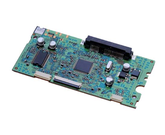
A multilayer printed circuit board combines outer and internal copper layers separated by insulating material and bonded into one board. Plated interconnections connect selected layers so the circuit can accommodate signal routing, power distribution and reference planes within a compact footprint.
Our multilayer PCB fabrication service covers 4–32-layer constructions. The right layer count depends on component density, routing requirements, electrical performance and mechanical constraints.
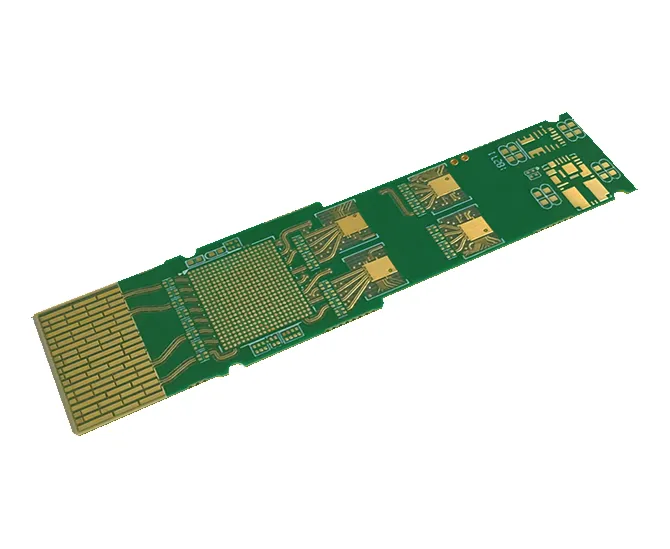
A multilayer PCB board does not automatically require HDI. Conventional plated through-holes can be suitable for many designs; microvias and sequential build-up are considered when component escape routing or interconnect requirements call for them.
Start with the construction you need
Rigid: fixed electronic assemblies and conventional multilayer routing.
Flexible: interconnects that need to fit around product geometry.
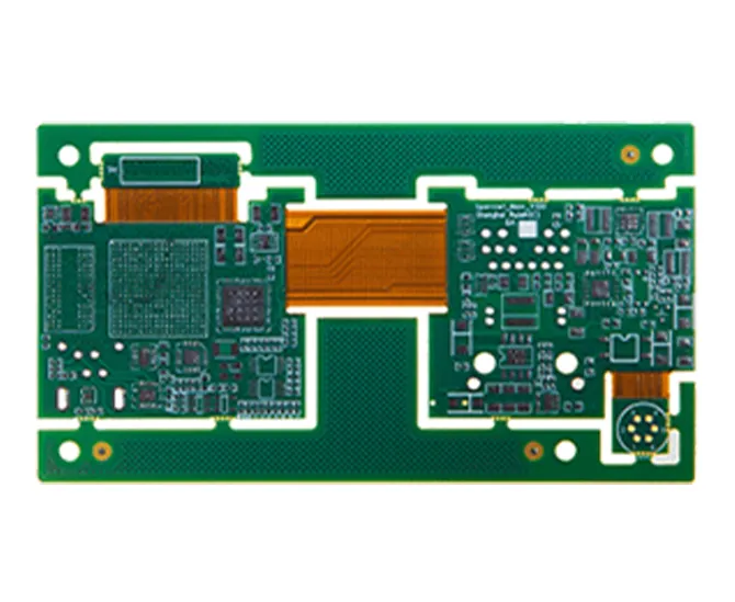
Rigid-flex: rigid mounting areas integrated with flexible connections.
Compare flexible PCB manufacturing, rigid-flex PCB construction and HDI PCB manufacturing.
China 365PCB Multilayer PCB Capabilities and Materials
Send your fabrication drawing and electrical requirements with the board files. We review the complete construction before confirming the production specification.
| Feature | 365PCB options | Project details to confirm |
|---|
| Copper layer count | 4–32 layers | Layer sequence, routing and plane allocation, board thickness and via structure. |
|---|
| Construction | Rigid, flexible and rigid-flex | Mechanical drawing, rigid and flex regions, local reinforcement and assembly requirements. Layer availability depends on construction. |
|---|
| Materials | FR-4, Rogers laminate options and polyimide | Exact grade, dielectric properties, thermal requirements and compatible bonding materials. |
|---|
| Stackup and copper | Project-specific layer build | Core and prepreg selection, finished copper by layer, dielectric spacing and total thickness tolerance. |
|---|
| Interconnections | Through-holes; blind, buried and microvia options | Via start/end layers, hole dimensions and any sequential lamination or filling requirements. |
|---|
| Fine-line features | Reviewed against the stackup | Required trace/space by layer and copper thickness. See our HDI fabrication capabilities for fine-line and microvia projects. |
|---|
| Impedance control | Controlled-impedance designs | Target values, tolerance, reference layers, trace geometry and coupon/report requirements. |
|---|
| Surface finish | Selected for the build | Finish type, pad function, assembly process and storage requirements. |
|---|
| Bare-board testing | 100% electrical testing | Continuity and isolation against the agreed board data; additional inspection and reporting as specified. |
|---|
| Assembly | Component sourcing, placement and testing | BOM, placement data, assembly drawing, programming and functional test scope. |
|---|
Choose the Layer Count Around the Circuit
More layers create routing and plane-placement options, but the best stackup is the one that meets the circuit’s requirements with manageable fabrication cost and complexity.
Evaluate whether the routing can be completed while retaining suitable reference planes, power distribution and manufacturing clearances.
Consider additional layers when pin count, multiple power domains or high-speed routing require more separation and reference-plane access.
Review high layer counts together with finished thickness, drilling, registration, material selection and test access.
Count copper layers, then define the dielectrics
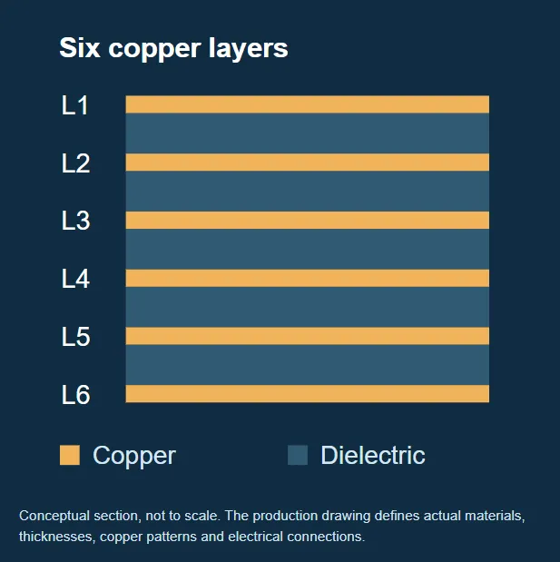
A six-layer multilayer circuit board has six conductive copper layers. Core and prepreg materials separate and bond the copper layers; solder mask and silkscreen do not add to the copper layer count.
The fabrication stackup also specifies dielectric thicknesses, copper weight and material grades. Two six-layer boards can have different impedance, finished thickness and manufacturing requirements.
Before routing: agree the layer sequence and usable materials.
Before ordering: release the final stackup, tolerances and via connections with the drawing.
Multilayer PCB Design and Stackup Support
A manufacturable multilayer PCB design coordinates electrical targets with the physical construction. We review the following items before the production data is released.
Signal and reference layers
Identify critical signals and their reference planes. Review return paths at layer changes and avoid routing sensitive signals across gaps in their reference plane.
Impedance requirements
Specify single-ended or differential targets, tolerance and controlled layers. Trace width, spacing, copper thickness and dielectric properties must be considered together.
Material selection
FR-4 is a common starting point. For RF, high-speed or flexible constructions, identify the required laminate grade and compatible bonding system.
Copper balance and thickness
Review copper distribution and dielectric balance around the stackup. Coordinate current-carrying needs with fine-line routing and finished board thickness.
Via and hole requirements
Define the layer span, drill data, pads and tolerances for each interconnection. Review blind or buried vias and microvias as distinct manufacturing features.
Manufacturing and assembly files
Provide Gerber and drill outputs with the fabrication drawing. For designs created in Altium, Cadence or Mentor Graphics, confirm native-file and version compatibility if a native project review is needed.
Separate impedance control from a full signal-integrity analysis
A controlled-impedance stackup addresses specified transmission-line structures. Full signal-integrity analysis may also require component models, connector data, interfaces, routing and operating conditions. Share the analysis scope so we can confirm the support required for your project.
Our Multilayer PCB Manufacturing Process
Multilayer PCB production follows the approved construction. Inner-layer circuitry is formed and inspected before bonding; drilling, plating and outer-layer work then complete the specified interconnections.
Confirm the drawing revision, layer stack, laminate system, copper requirements, holes, impedance targets and acceptance criteria.
Form the internal copper patterns and inspect them before lamination makes those surfaces inaccessible.
Align the specified cores, bonding materials and copper foils. Apply the bonding process required for the selected material system.
Form holes and plated connections according to the released drill data. Blind, buried and HDI structures may require operations at intermediate stages.
Complete outer-layer patterns, solder-mask openings, surface finish, identification and board profiling.
Test bare boards for continuity and isolation, complete the agreed inspections, then release the boards for shipment or component assembly.
For specialist interconnections, explore blind via PCB construction and HDI PCB fabrication.
Quality Control for Multilayer Printed Circuit Boards
365PCB provides 100% bare-board electrical testing. We also agree the dimensional, structural and reporting requirements needed for your order, including applicable IPC acceptance criteria.
| Inspection stage | What the check addresses | Order requirements to agree |
|---|
| Inner-layer inspection | Copper-pattern defects and alignment before the layers are bonded. | Critical features and inspection coverage before lamination. |
|---|
| Dimensional and structural checks | Outline, thickness, registration and selected internal features. | Tolerances and any microsection, plating or lamination assessment required. |
|---|
| Bare-board electrical testing | Continuity and isolation against the agreed netlist or board data. | Electrical acceptance criteria, traceability and test records. |
|---|
| Impedance verification | The specified controlled-impedance structures or representative coupons. | Target values, tolerance, coupon design and measurement report. |
|---|
| Assembly AOI / X-ray | Component placement, visible solder joints and selected hidden connections after assembly. | Inspection method, applicable features and acceptance criteria. |
|---|
| Functional or reliability testing | Defined assembled-board functions or behavior under specified stress conditions. | Test procedure, fixtures, operating conditions, sampling and reporting scope. |
|---|
Electrical testing checks bare-board connectivity. It does not replace functional testing of the populated circuit or qualification for its operating environment.
Applications of Multilayer PCBs
Multilayer construction supports products that need more routing space, reference planes or power distribution than a simpler board can provide. Select the stackup and qualification plan around the actual circuit.
Telecom and networking
Communication modules and networking equipment with dense interfaces, controlled-impedance routing and defined material requirements.
Telecommunication PCB manufacturingServers and computing
High-pin-count devices, memory interfaces and multiple supply rails that require coordinated routing and plane allocation.
High-speed PCB manufacturingMedical equipment
Imaging, diagnostic and monitoring electronics with project-specific documentation, traceability and acceptance requirements.
Medical PCB requirementsAerospace electronics
Control and avionics assemblies where materials, interconnect reliability and environmental qualification are defined for the product.
Aerospace PCB project supportAutomotive and industrial control
Controllers and interface boards that need coordinated power distribution, signal routing and operating-environment requirements.
Automotive PCBs
Industrial control PCBs
IoT and connected devices
Compact sensing and communication assemblies where component density and enclosure space guide the construction.
IoT and edge-device assembly
 English