





TY_HOME14
China 365PCB Technology Co., Ltd.
  • high speed pcb
  • high speed pcb

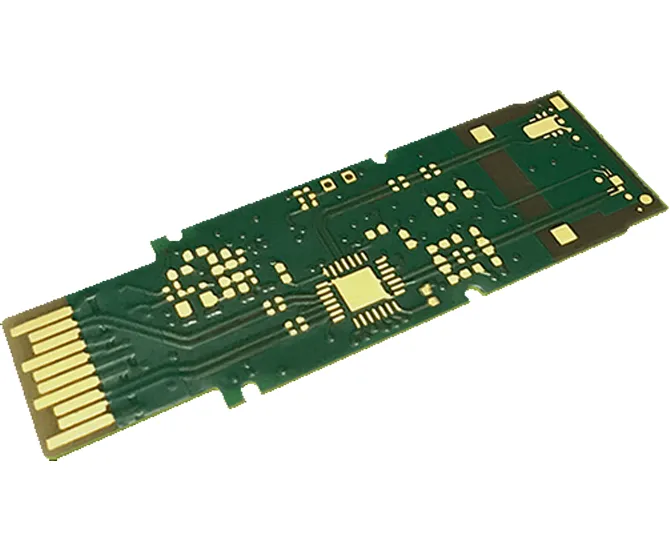
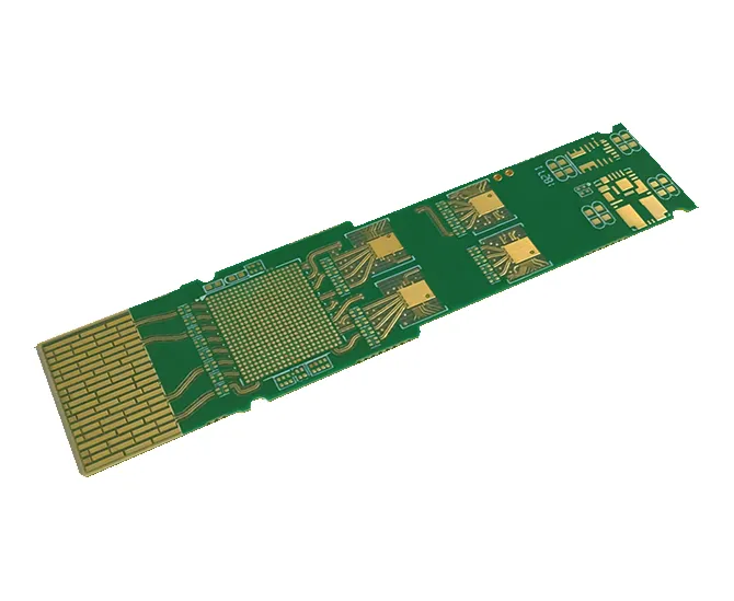
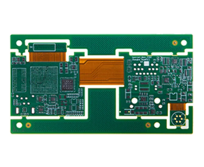
High-speed PCB

At China 365PCB, we specialize in the design, fabrication, and assembly of High-Speed Printed Circuit Boards (PCBs) that are critical for next-generation digital and RF systems. Backed by our advanced PCB manufacturing services, we deliver high-precision boards with consistent quality and performance for demanding high-speed applications. Our manufacturing expertise ensures precise impedance control, minimized signal loss, and superior electromagnetic performance—delivering the foundation your high-speed designs demand for reliable, first-pass success.

Our Core Capabilities

Advanced Materials & Substrates365PCB works with industry-leading low-loss, low-Dk/Df laminates (including Rogers, Taconic, Isola, Panasonic Megtron 6/7, and Nelco) to perfectly meet your specific high-signal-speed, multi-gigabit performance, and rigorous thermal management requirements.

Precision Impedance Control & VerificationWe guarantee ultra-tight impedance tolerances (typically ±10%, down to ±5% upon request) for single-ended and differential pairs. This is achieved through strictly controlled dielectric thickness, ultra-precise copper trace geometry, and advanced simulation-backed stackup manufacturing processes.

High-Density Interconnect (HDI) IntegrationExpert engineering for complex layouts, utilizing laser microvias, stacked/blind/buried vias, and fine-line tracing (down to 2/2 mil mil line/space) to seamlessly support high-pin-count, fine-pitch BGAs (0.4mm pitch and below) and advanced chip-scale packages common in high-speed hardware design.

Comprehensive Signal & Power Integrity SupportOur proactive in-house DFM analysis targets high-speed bottlenecks upfront—minimizing EMI/crosstalk, optimizing return paths, managing trace skew, and ensuring robust power integrity. All processes are cross-optimized with our turnkey PCB assembly services to guarantee a seamless transition from prototyping to mass production workflow.

Key Technologies & Features

Back Drilling (Controlled Depth)
Precisely removes unwanted via stubs to completely eliminate signal reflections, crucial for maintaining signal integrity at 28Gbps, 56Gbps, and higher multi-gigabit rates.
Any-Layer HDI & Via-in-Pad
Provides ultimate routing flexibility, reducing layout space, minimizing parasitic inductance, and optimizing performance in extremely dense, space-constrained, high-frequency layouts.
Stripline & Microstrip Configurations
Advanced layer stack-up construction engineered specifically for controlled impedance transmission lines, maintaining uniform RF environments throughout the entire PCB substrate.
Advanced Surface Finishes
Full availability of high-tier surface plating options including ENIG, ENEPIG, Immersion Silver, Immersion Tin, and Hard Gold to perfectly suit different operating signal frequencies and assembly requirements.

Typical Applications

✔ 5G/6G Communication Infrastructure (Base Stations, RF Power Modules)✔ High-Performance Computing (HPC) & Enterprise Data Center Hardware✔ AI/ML Hardware Accelerators, Advanced GPU & FPGA Motherboards
✔ High-Speed Networking Devices & Optical Transceivers (400G/800G+)✔ Next-Gen Automotive Systems (ADAS, RADAR & LiDAR Systems)✔ High-Frequency Test & Precision Measurement Equipment

Dedicated Engineering & Support Team

* Your Name
* E-mail Address
* Contact Phone
* Company Name
* Message Content
We use cookies to offer you a better browsing experience, analyze site traffic and personalize content. Part of the tracking is necessary to ensure SEO effectiveness,
By using this site, you agree to our use of cookies. Visit our cookie policy to learn more.

Reject Accept