What is a rigid-flex PCB?
One laminated circuit across rigid and bendable regions
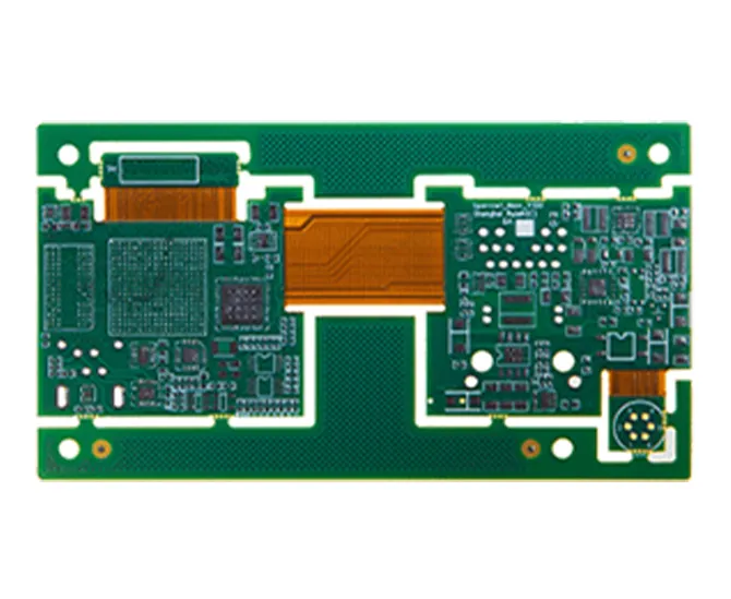
A rigid-flex PCB is a printed circuit in which rigid board sections and flexible circuit sections are integrated into one finished part. Copper layers continue through selected regions of the construction, allowing the flex section to fold or move while the rigid areas support components, connectors and mechanical attachment.
This is different from connecting independent rigid boards with a removable cable. A properly planned rigid and flexible PCB can reduce connector count, save assembly space and control interconnect geometry, but the benefit depends on a stackup and mechanical design developed for the real bend condition.
As a rigid flex PCB manufacturer and rigid flex PCB supplier, 365PCB supports design review, rigid flex PCB fabrication, bare-board testing and optional assembly. Projects can also draw on our broader PCB manufacturing capabilities and PCB design support services.
Rigid flex PCB manufacturing capabilities
The table below is a practical starting point. Final producibility is determined from the complete regional stackup, finished thicknesses, via structure, flex geometry, material availability and inspection plan.
| Item | Typical capability | What to define in the RFQ |
|---|
| Layer count | 4–12 total copper layers | Identify the layers present in each rigid region and the layers that continue through every flex region. |
|---|
| Materials | Polyimide flex core with FR-4 rigid sections | Include finished thickness, copper weight, coverlay and bonding requirements. Specialty materials are reviewed by stackup. |
|---|
| Via structures | Plated through holes, blind/buried vias and laser microvias, subject to stackup | Mark via types, target layers, filled/capped requirements and any via-in-pad locations. |
|---|
| Impedance control | Single-ended and differential structures by engineering review | Provide target impedance, tolerance, reference layer, trace geometry and coupon or report requirement. |
|---|
| Flex-region features | Coverlay, selective stiffeners, local reinforcement and EMI shielding options | Show flex boundaries, stiffener outlines, thickness, shielding termination and adhesive keepouts. |
|---|
| Surface finish | Selective finish options based on exposed pad and connector functions | Identify solderable pads, contact fingers, mating areas and any thickness requirements. |
|---|
| Acceptance criteria | IPC-6013 Class 2 or Class 3 project requirements can be reviewed | State the required class, applicable drawing notes, sampling plan and any customer-specific criteria. |
|---|
| Production scope | Rigid-flex PCB prototype through volume production, with optional assembly | Provide prototype and forecast quantities so tooling, panelization and sourcing can be planned together. |
|---|
Specify What Exists in Each Part of the Board
A rigid-flex stackup must describe more than the total layer count. In many designs, only selected copper layers continue through the flexible span while additional copper and dielectric layers build the rigid component areas. The flex-to-rigid transition also needs its own definition because material and copper edges create local changes in stiffness.
| Region | Key definition |
| Rigid area | Layer sequence, FR-4 thickness, copper weight, via span, component side and finished thickness. |
| Transition zone | Rigid material edge, coverlay overlap, adhesive condition, copper features, routing clearance and strain-relief geometry. |
| Flex area | Flex layers, polyimide and coverlay thickness, bend direction, bend radius, shielding and dynamic or static use. |
Important: “12-layer rigid-flex PCB” describes the total construction; it does not automatically mean that all 12 copper layers pass through every bendable region.
Rigid-flex PCB Fabrication Process
Manufacturing is planned as a controlled sequence so the flexible core, rigid build-up, via structures and exposed flex areas remain registered through lamination and finishing.
Engineering and DFM review
Flex circuitry and coverlay
The flexible copper circuitry is formed, inspected and aligned with coverlay openings, stiffener locations and the defined transition geometry.
Rigid-flex layup and lamination
Flex cores, rigid materials, copper foils and bonding layers are registered and laminated according to the approved construction.
Drilling, plating and build-up
- Outer circuits, solder mask in rigid areas, selective finish, legend and final profiling are completed while protecting exposed flex sections.
- Inspection and release
Electrical testing and the agreed visual, dimensional, microsection or impedance checks are completed before shipment or assembly.
Projects with dense interconnects can combine rigid-flex construction with HDI PCB technology, laser-drilled microvias and sequential lamination. The number of build-up cycles and microvia structure should be agreed before layout completion.
Rigid Flex PCB Applications
Rigid-flex construction is most useful when connector elimination, repeatable folding, low mass or packaging into multiple planes creates a measurable system advantage.
Navigation electronics, sensors and compact modules where vibration, mass and interconnect retention must be considered together.
Portable diagnostics, compact instruments and sensor assemblies that require controlled packaging and documented acceptance criteria.
Wearables, cameras and foldable or space-constrained products with circuit sections arranged across multiple planes.
Cameras, displays, controls and sensor modules where connectors and wiring must fit within restricted spaces.
Robotics, motion-control assemblies and instrumentation with moving sections or constrained internal routing.
Compact communication and control assemblies produced to the drawings, test conditions and documentation required by the project.
Rigid flex PCB assembly under One Project
Rigid-flex PCB assembly requires mechanical support for thin flex tails and transition areas during printing, placement, reflow, handling and inspection. Tooling strategy, panel retention, stiffener thickness and component-side definition should be reviewed before the bare boards are released.
365PCB can combine fabrication with component sourcing, SMT assembly, BGA placement and project-defined testing. X-ray inspection is used where hidden assembled solder joints require evaluation; it is not a substitute for bare-board electrical testing.
For a complete PCBA review, see our dedicated flex and rigid-flex PCB assembly service, general PCB assembly services, and BGA and fine-pitch assembly capabilities.
FAQs About Rigid flex PCB
Q1: Do you support 10-layer rigid-flex PCB manufacturing?
A: Yes, we manufacture 4–12 layer rigid-flex PCBs with precise stack-ups and impedance control.
Q2: What materials are used in your flexible circuit boards?
A: We use polyimide, PET, and FR4 combinations for rigid-flex and flexible PCBs.
Q3: Can rigid-flex PCBs support fine-pitch components like BGA?
A: Yes, we support HDI rigid-flex PCBs with laser-drilled microvias and BGA compatibility.
Q4: Do you have IPC Class 3 rigid-flex PCB capability?
A: Yes, we are IPC Class 3 certified, suitable for high-reliability applications.
Q5: What's the lead time for a multilayer rigid-flex PCB prototype?
A: Typically 7–9 days depending on the layer count and complexity.
 English