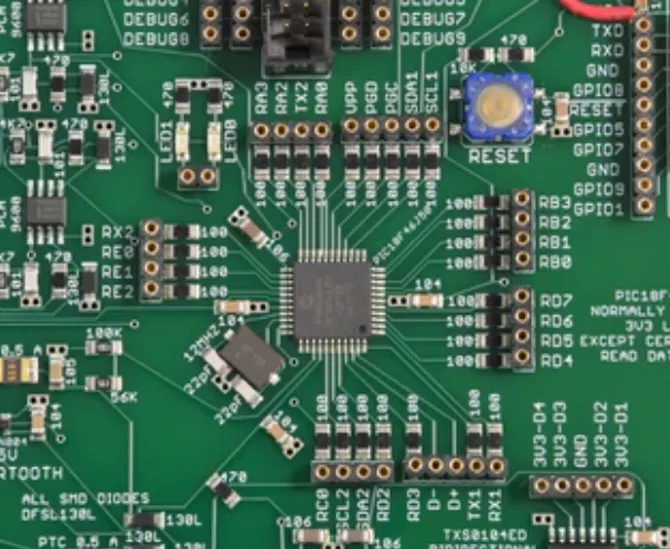
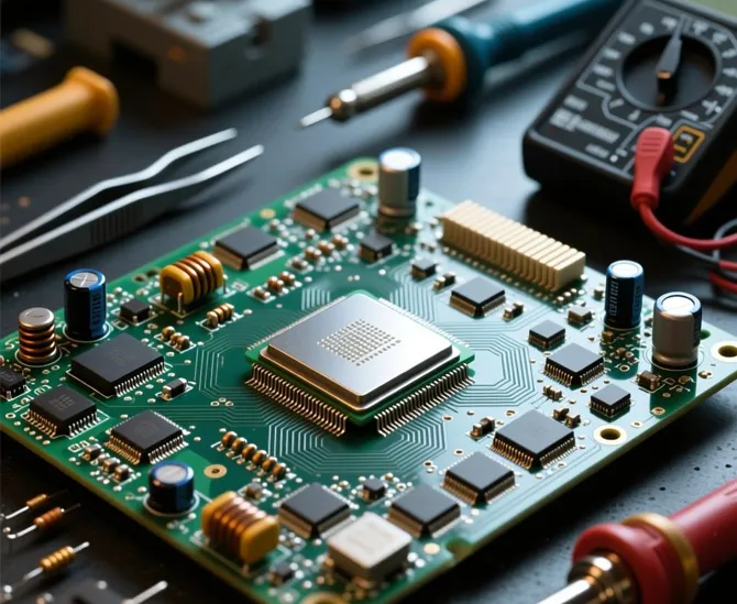
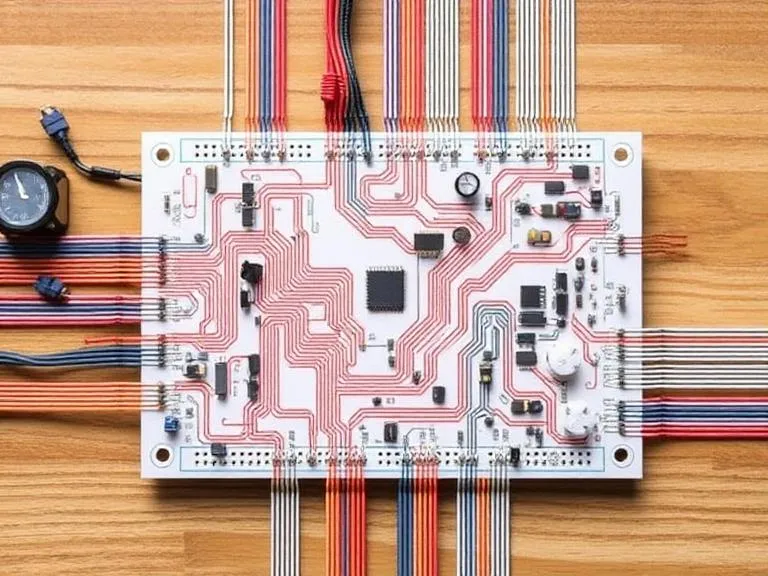
Hardware engineering has a dirty secret: an alarming amount of early-stage product development relies on tangled masses of copper wire, burnt fiberglass, and unreliable solder joints. When engineers or electronics hobbyists ask about a PCB prototype board how to use and master it, they are usually referring to traditional perfboards or stripboards. These pre-drilled, bare-bones boards serve as the immediate physical bridge between a schematic on a computer screen and a tangible, working electronic circuit.
From our experience as a leading manufacturer at China 365PCB, relying too heavily on manual prototype boards for anything beyond simple low-speed logic testing is a catastrophic waste of engineering hours. The industry has aggressively shifted. While knowing how to cut, populate, and point-to-point solder a perfboard is a fundamental rite of passage for any electrical engineer, relying on this method for modern high-speed or radio frequency applications will ruin your signal integrity. In this guide, we provide uncompromising, practical instructions on how to effectively use manual PCB prototype boards, while also explaining exactly when you must abandon them in favor of custom, rapid-turnaround fabricated boards to achieve commercial viability.
Quick Answer: How to Use a PCB Prototype Board
To successfully build a circuit on a manual PCB prototype board (perfboard or stripboard), follow these precise steps:
Schematic Translation: Map your digital schematic to a physical grid using breadboard layout software or graph paper.
Component Placement: Insert through-hole components from the non-copper side (top), bending the leads outward at a 45-degree angle on the copper side (bottom) to mechanically anchor them.
Trace Planning: If using a stripboard, use a spot face cutter or drill bit to break the continuous copper tracks where electrical isolation is required.
Point-to-Point Soldering: Solder the component leads to the copper pads. Use 22-24 AWG solid core wire or solder bridges to connect adjacent pads according to your schematic.
Continuity Testing: Use a digital multimeter on the continuity setting to verify all connections and ensure no unintended solder bridges (shorts) exist before applying power.
Note for Commercial Development: Manual prototyping is strictly for low-frequency, initial proof-of-concept work. For any project requiring surface mount devices (SMD), controlled impedance, or professional validation, you must graduate to a custom PCB Prototype Service.
What It Is: The Anatomy of Prototype Boards
A manual PCB prototype board—often referred to interchangeably as a perfboard, dot PCB, or stripboard—is a rigid sheet of insulating material, typically FR2 (phenolic paper) or standard FR4 PCB fiberglass, pre-drilled with a grid of holes spaced exactly 0.1 inches (2.54 mm) apart. This spacing universally matches the lead pitch of standard through-hole electronic components, such as DIP (Dual In-line Package) integrated circuits, resistors, and capacitors.
The distinction between board types is critical. A perfboard features individual, isolated copper pads surrounding each hole. You must physically create the electrical connections between components using wire or solder bridges. A stripboard (or Veroboard) features continuous parallel tracks of copper connecting rows of holes. This allows you to place components along a shared bus line, but requires you to physically cut the copper track with a cutting tool whenever you need to interrupt the circuit.
How It Works: Execution and Soldering
In most professional situations, the transition from a solderless breadboard to a soldered perfboard is the first step in ruggedizing a proof-of-concept. The process demands meticulous mechanical and thermal execution.
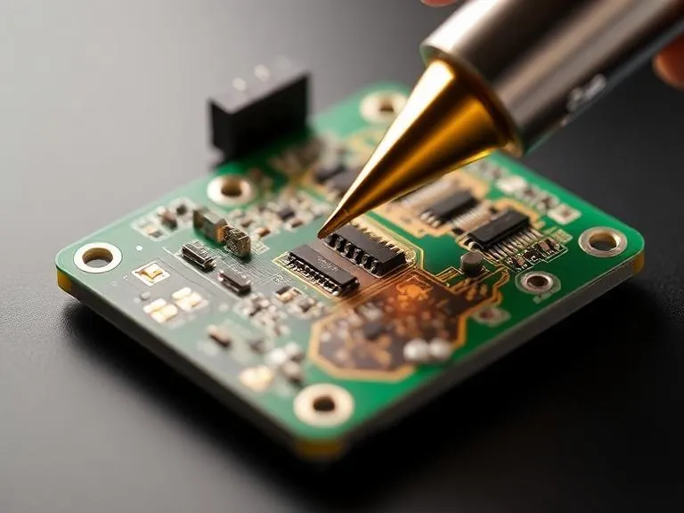
First, always populate the lowest-profile components (resistors, diodes) before moving to taller components (capacitors, relays, heat sinks). This allows you to flip the board upside down on your workbench without the components falling out. Once inserted, splay the leads slightly to hold them in place. When soldering, apply a temperature-controlled iron (typically set between 350°C and 380°C for lead-free solder) simultaneously to the copper pad and the component lead. Feed rosin-core solder directly into the heated joint, allowing it to flow and form a concave, shiny cone. Remove the heat and allow the joint to cool undisturbed to prevent a brittle "cold" solder joint.
To route signals on a perfboard, you must execute point-to-point wiring. Strip the ends of solid-core hookup wire, wrap it around the component leads, and solder it down. For adjacent pads, you can drag a bead of solder across them to create a bridge, though this requires high-quality flux to manipulate the surface tension of the molten metal.
The True Benefits of Manual Prototyping
The sole overriding benefit of a manual PCB prototype board is immediate physical gratification. If you have an idea for a simple analog audio filter or a basic LED driver array, you can assemble, solder, and test it within an hour using components from your bin. There are no computer-aided design (CAD) files to generate, no manufacturing lead times to wait for, and the material cost is negligible. It provides a permanent, vibration-resistant circuit compared to the notoriously flaky connections of a solderless plug-in breadboard.
Severe Limitations You Cannot Ignore
We must use commercial and practical judgment: manual prototype boards are functionally obsolete for 90% of modern hardware engineering. The limitations are insurmountable for advanced electronics.
First, consider signal integrity. When you use long, unshielded jumper wires to connect components, you introduce massive parasitic inductance and capacitance. If you attempt to build a switching power supply or route data over a manual board, the resulting electromagnetic interference (EMI) and crosstalk will render the circuit unstable. In our testing, attempting to validate a High-Frequency PCB design or a Radio Frequency PCB layout on a stripboard is mathematically impossible; the geometry of the physical traces cannot be controlled to match specific impedance requirements (like 50 ohms).
Secondly, manual boards are strictly designed for through-hole technology (THT). Today, over 95% of active microprocessors, sensors, and power management ICs are manufactured exclusively in surface-mount device (SMD) packages (e.g., QFN, BGA). You cannot easily mount a 0.4mm pitch BGA chip onto a perfboard without relying on cumbersome and unreliable breakout adapter boards.
Who Should Use Manual Boards
For beginners, university students, and hobbyists building low-frequency analog circuits, power distribution boards for robotics, or basic micro-controller shields, perfboards are the perfect educational tool. They teach fundamental soldering skills, spatial planning, and basic circuit troubleshooting.
Who Does Not Need Them
For commercial users, hardware startups, and professional engineers, wasting three days hand-soldering a messy perfboard is a terrible allocation of resources. Your time is worth vastly more than the cost of a fabricated board. If you are developing consumer electronics, industrial controllers, or IoT devices, you must bypass manual boards and move directly from breadboard to a fabricated prototype.
Common Mistakes in Prototyping
The most catastrophic mistake developers make on manual boards is poor thermal management. Running high current through a thin gauge jumper wire or a tiny solder bridge will cause the board to overheat, delaminate, and potentially catch fire. If your circuit requires handling more than a few amps, you cannot rely on thin copper tape or 24 AWG wire; you must design a proper Heavy Copper PCB with mathematically calculated trace widths.
Another profound error is the "spaghetti wiring" syndrome. Routing wires haphazardly across the board makes debugging impossible. If a circuit fails, tracing a single signal through a nest of identical-colored wires is an exercise in futility. Always color-code your wiring (e.g., red for VCC, black for GND, yellow for signal) and route wires in neat, 90-degree angles flat against the board.
Buying Considerations for the Next Step
When you have validated your basic logic and are ready to graduate from a manual perfboard to a commercially fabricated prototype, your buying considerations must shift toward manufacturability and environmental resilience. You must transition from standard phenolic paper to specialized laminates.
If your device operates in extreme temperature environments, you must specify a High TG PCB material to prevent the board from warping under thermal stress. If your design requires complex routing that cannot fit on two layers, you will need to specify a multi-layer HDI PCB (High Density Interconnect) utilizing a Laser Drilled PCB process for microvias. Furthermore, dictate your surface finish carefully. Bare copper oxidizes rapidly; specify an ENIG(Electroless Nickel Immersion Gold)PCB finish for perfectly flat pads that guarantee optimal solderability for your fine-pitch surface mount components.
Expert Recommendation
We recommend a hard cut-off for manual prototyping. Use a perfboard solely to prove that an isolated sub-circuit functions at a basic level. Once the core logic is validated, stop hand-soldering. Open your EDA software (Altium, KiCad, or Eagle), route your PCB, and utilize a quick-turn assembly service. The modern hardware development cycle demands iteration speed and precise electrical characteristics that human hands simply cannot replicate with a spool of wire.
China 365PCB Prototype PCB Assembly
Fast and affordable prototype PCB assembly services with no MOQ. Ideal for hardware development, product validation, and engineering test runs.
At China 365PCB, we specialize in prototype PCB assembly for startups, engineers, and hardware developers looking for quick-turn, low-volume production to test and validate their designs. Our prototype services are tailored for fast iterations, with options including SMT, THT, BGA, and mixed technology assembly. We use automated SMT lines, expert manual soldering, and precise DFM/DFA checks to ensure that your PCB prototype assembly is delivered accurately, tested, and ready for functionality evaluation. Whether it’s your first design or a pre-production run, China 365PCB is your ideal partner.
Start Your Custom Prototype TodaySummary and Comparison Tables
Quick Summary Table: Types of Prototyping Boards| Board Type | Primary Characteristic | Best Use Case |
|---|
| Breadboard | Solderless, plug-and-play spring clips. | Temporary testing, learning, rapid component swapping. |
| Perfboard | Isolated copper pads, requires point-to-point wiring. | Permanent, custom analog circuits, one-off hobby projects. |
| Stripboard (Veroboard) | Continuous copper tracks, requires trace cutting. | Circuits with heavy shared buses (power/ground lines). |
| Custom Fabricated PCB | Etched copper traces, solder mask, silkscreen. | Commercial prototypes, high-speed data, SMD components. |
Comparison Table: Manual Perfboard vs. Custom Fabricated PCB| Feature | Manual Perfboard | Custom Fabricated PCB |
|---|
| Turnaround Time | Instant (Start building immediately) | 24 Hours to 5 Days (Depending on service) |
| Signal Integrity | Very Poor (High EMI, unpredictable impedance) | Excellent (Controlled via software design) |
| SMD Compatibility | Extremely Difficult (Requires breakout boards) | Native (Perfect for BGA, QFN, 0201 packages) |
| Labor Cost | Extremely High (Hours of manual point-to-point wiring) | Low (Automated pick-and-place assembly) |
| Reproducibility | Zero (Every hand-built board is unique and flawed) | 100% (Identical mechanical and electrical copies) |
Pros and Cons Table: Hand-Soldered Prototype Boards| Pros (Advantages) | Cons (Limitations) |
|---|
| Lowest possible upfront financial cost for a single unit. | Aesthetically unprofessional for investor or client demos. |
| No specialized CAD or gerber file generation required. | Massive risk of human error (cold solder joints, accidental shorts). |
| Allows for physical, on-the-fly circuit modification and hacking. | Impossible to implement complex form factors like a Bendable PCB or Rigid Flex PCB. |
| Excellent medium for training junior technicians in soldering basics. | Lacks proper thermal relief, making Aluminum PCB or Metal Core PCB heat dissipation impossible. |
Frequently Asked Questions
Can I use surface mount (SMD) components on a standard perfboard?
Technically yes, but it is highly impractical. Standard perfboards are drilled at a 2.54mm pitch, which is designed exclusively for through-hole components. To use an SMD chip, you must purchase a specific "breakout board" adapter, solder the SMD chip to the adapter, and then solder the adapter's header pins into the perfboard. This adds unnecessary cost, height, and potential failure points to your prototype.
How do you cut a PCB prototype board to the correct size?
The cleanest method to cut a fiberglass (FR4) perfboard is by deeply scoring it with a heavy-duty utility knife along a metal straight-edge on both sides, then snapping it cleanly over the edge of a table. You can also use a rotary tool (like a Dremel) with a diamond cutting wheel, or a small hacksaw. Always wear a respirator and safety glasses when cutting FR4, as inhaling airborne fiberglass dust is hazardous to your respiratory system.
What is the best wire to use for point-to-point soldering on a perfboard?
For signal routing on a perfboard, we recommend using 22 AWG or 24 AWG solid-core tinned copper wire, often referred to as "bus wire" or "hookup wire." Solid-core wire holds its shape when bent, allowing you to route traces flat against the board neatly. Do not use stranded wire for point-to-point trace routing, as the individual strands can easily fray, cross over to adjacent pads, and cause devastating short circuits.
Authoritative Industry References
To ensure engineering accuracy and compliance with global manufacturing standards, the mechanical and electrical principles discussed in this guide reference the following authoritative bodies:
For more advanced integration, such as combining rigid logic boards with dynamic mechanical sections, explore the engineering behind a Flex-Rigid Board.
David Li
David Li is the Technical Communications Director at China 365PCB, with over 15 years of hands-on experience in the PCB and electronics manufacturing industry. Holding a Master’s degree in Electrical Engineering, he has worked extensively in both R&D and manufacturing roles at leading multinational electronics firms in Shenzhen before joining our team.
His expertise spans high-speed digital design, advanced packaging (HDI, Flex), and automotive-grade reliability standards. David is passionate about bridging the gap between design intent and production reality—a philosophy that aligns perfectly with 365PCB’s mission to deliver seamless, rapid, and fully-integrated manufacturing solutions.
Follow David’s insights on PCB technology trends and best practices here on the 365PCB Knowledge Hub.
 English