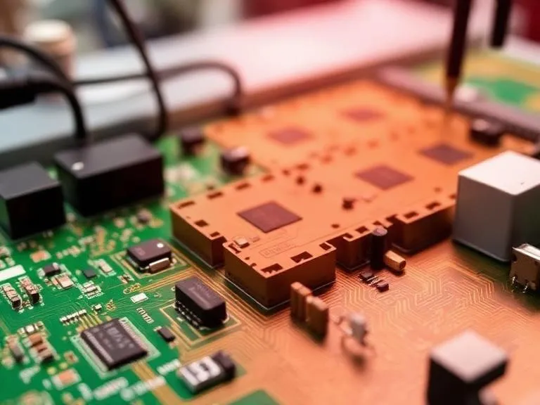
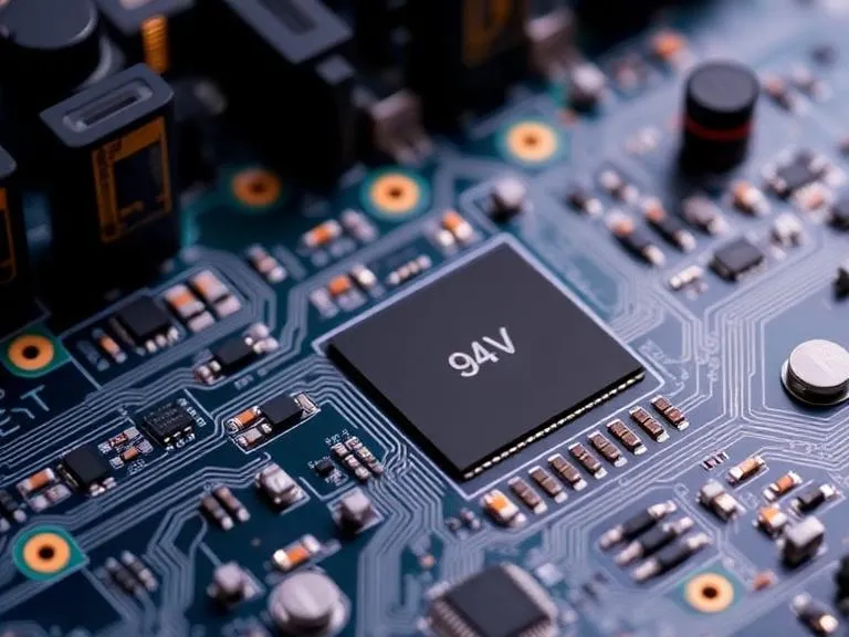
Every modern electronic device, from the smartphone in your pocket to the complex navigation systems of commercial aircraft, relies on a foundational substrate to route electrical signals and power. At the absolute core of this electronic ecosystem is the printed wiring board. Understanding what a printed wiring board is, how it is manufactured, and where it is applied is essential for mechanical engineers, electrical designers, and hardware procurement specialists.
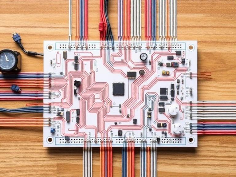
As China 365PCB, a fully self-operated, full-industry-chain manufacturing group with over 15 years of experience, we have engineered and manufactured millions of these critical components. Operating over 100,000 square meters of production area, our self-owned and self-managed facilities ensure total quality control, full process traceability, and unmatched production flexibility. In this comprehensive guide, we will provide a deep technical dive into the printed wiring board, exploring its materials, fabrication processes, industry applications, and how it differs from associated terminology.
1. The Core Definition: What is a Printed Wiring Board?
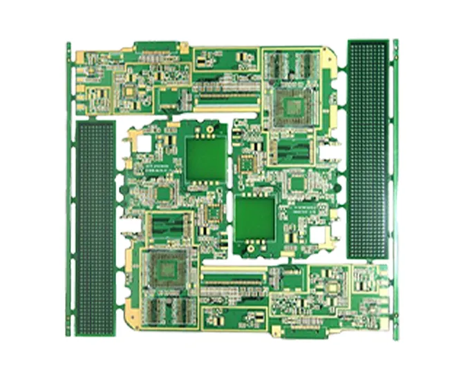
A printed wiring board (often abbreviated as PWB) is a non-conductive substrate upon which conductive pathways, tracks, and signal traces are etched or printed from copper sheets. The primary function of a printed wiring board is to provide both mechanical support and a highly organized electrical routing system for electronic components.
Historically, before the advent of surface mount technology and automated component assembly, the industry relied on point-to-point chassis wiring. This was bulky, error-prone, and impossible to scale for mass production. The invention of the printed wiring board revolutionized electronics by allowing engineers to "print" the wire directly onto a flat board. Today, a printed wiring board serves as the blank canvas of an electronic assembly—it is the bare board prior to the attachment of resistors, capacitors, integrated circuits, and other electronic components.
2. The Anatomy of a Printed Wiring Board
To fully grasp how a printed wiring board functions under mechanical and thermal stress, we must look at its cross-sectional anatomy. From our experience in high-reliability fabrication, the structural integrity of these layers determines the overall lifespan of the hardware.
The Base Substrate (Dielectric Layer)
The core of any printed wiring board is the dielectric substrate. The most common material used is FR-4, a glass-reinforced epoxy laminate that is highly flame retardant. This material provides the necessary rigidity and electrical insulation to prevent signal shorting between copper layers.
The Conductive Copper Layers
Laminated onto the substrate is a thin layer of copper foil. Depending on the complexity of the design, a printed wiring board can be single-sided (one copper layer), double-sided (two copper layers), or multi-layered (four to over sixty layers). Multi-layer boards utilize prepreg materials to separate internal copper routing planes.
The Solder Mask
The characteristic green (or sometimes blue, black, or red) color of a printed wiring board comes from the solder mask. This is a polymer layer applied over the copper traces to protect them from oxidation and to prevent solder bridges from forming between closely spaced pads during the assembly process.
The Silkscreen
The final layer applied to a printed wiring board is the silkscreen. This layer contains text, logos, component identifiers, and warning symbols. It is essential for guiding automated assembly machines and human technicians during the subsequent component placement phases.
3. Printed Wiring Board Manufacturing Process
The fabrication of a printed wiring board is a complex chemical and mechanical process. At China 365PCB, we utilize advanced automation to ensure every board meets strict IPC standards. We recommend a thorough understanding of this process for engineers looking to optimize their designs for manufacturability.
First, the digital Gerber files are processed by our CAM engineering team. The bare substrate, clad in copper, undergoes a photolithography process where a photoresist material is applied and exposed to UV light through a film mask. The board is then passed through a chemical etching solution, which removes the unprotected copper, leaving behind the precise conductive pathways of the printed wiring board.
For multi-layer designs, these individual layers are meticulously aligned and laminated together under intense heat and hydraulic pressure. Following lamination, high-speed CNC drills create the vias and through-holes. These holes are then chemically plated with copper to ensure electrical conductivity between the different layers of the printed wiring board. Finally, the solder mask and silkscreen are applied, and the board undergoes strict electrical testing, such as flying probe or bed-of-nails testing, to verify continuity and isolation.
4. Printed Wiring Board vs. Printed Circuit Board: Clarifying the Terminology
One of the most frequent questions we encounter from new procurement teams is the difference between a printed wiring board (PWB) and a printed circuit board (PCB). While the terms are frequently used interchangeably in modern engineering vernacular, they have distinct technical definitions.
A printed wiring board refers specifically to the bare, unpopulated substrate with its copper routing network. It is strictly the "wiring" aspect of the board. However, once electronic components are soldered onto the printed wiring board, it officially becomes a printed circuit board (PCB) or a printed circuit board assembly (PCBA). In essence, every PCB begins its life as a printed wiring board. The distinction is primarily rooted in legacy military and aerospace terminology, where precise component definitions are mandatory for documentation.
5. Industry Applications of the Printed Wiring Board
The versatility of the printed wiring board means it must be engineered to withstand a vast array of environmental factors. From extreme vibration to high thermal loads, the application dictates the manufacturing parameters.
In heavy factory automation and robotic systems, substrates must withstand continuous mechanical vibration and electrical noise. For these environments, we engineer specific high-reliability layouts found in an Industrial Control PCB. These boards utilize heavy copper and thick FR-4 to guarantee stability.
Modern 5G networks and satellite communications rely on high-frequency signal transmission. To prevent signal loss, a printed wiring board in this sector requires low dielectric constant materials like PTFE. This is the foundation of a high-performance Telecommunication PCB.
Thermal management is the most critical factor for lighting systems. Because high-power diodes generate significant heat, a printed wiring board designed for this sector often utilizes an aluminum or metal-core base to dissipate heat efficiently, which is the hallmark of an LED Lighting PCB.
The renewable energy sector demands electronics that can operate outdoors for decades. High voltage and high current require specialized trace widths and heavy copper weights, typical of a robust Solar PCB utilized in solar inverters and battery management systems.
The automotive industry's shift toward electrification requires a printed wiring board that can handle extreme temperature cycling and mechanical shock. Flexible and rigid-flex board designs are frequently deployed as an EV PCB for battery monitoring and powertrain control.
In flight technology, there is zero margin for error. A printed wiring board destined for orbit or commercial flight undergoes rigorous outgassing tests and utilizes polyimide materials to ensure the structural integrity of an Aerospace PCB.
Finally, for mission-critical tactical hardware, encrypted communication devices, and radar systems, strict adherence to MIL-PRF-31032 standards is required. We manufacture highly specialized substrates to function flawlessly as a Military PCB.
6. Material Selection and Design Considerations
From our experience, the failure of a printed wiring board in the field is rarely due to a manufacturing defect, but rather a mismatch between the chosen base material and the operational environment. We recommend that engineers carefully calculate the Glass Transition Temperature (Tg) of their selected laminate.
For standard consumer electronics, a standard Tg (around 130°C) is perfectly acceptable. However, for industrial, automotive, and aerospace applications, high-Tg materials (170°C and above) are absolutely necessary. When a printed wiring board is subjected to temperatures exceeding its Tg, the resin matrix begins to expand rapidly in the Z-axis, which can fracture the copper plating inside the vias, leading to catastrophic intermittent electrical failures.
7. Why Choose China 365PCB for Your PWB Needs?
Selecting a manufacturing partner for your printed wiring board requirements is a critical supply chain decision. China 365PCB stands apart as a fully self-operated, full-industry-chain manufacturing group. We do not outsource our core competencies. From bare printed wiring board fabrication and SMT assembly to online electronic component sourcing, CNC machining, and cable harness assembly, we provide complete OEM/ODM solutions under one roof.
With 15+ years of dedicated industry experience and operating over 100,000 square meters of self-owned production area, we offer our clients unparalleled process traceability. Our massive scale ensures high production flexibility, whether you require rapid prototyping of a complex 24-layer printed wiring board or mass production of single-sided aluminum boards.
8. Summary Table: Printed Wiring Board Essentials
| PWB Characteristic | Standard Specification / Function | China 365PCB Engineering Recommendation |
|---|
| Base Substrate | FR-4, Aluminum, Polyimide, PTFE | Select high-Tg FR-4 for industrial environments to prevent thermal expansion failures. |
| Copper Weight | 0.5 oz to 2.0 oz (Standard) | Use heavy copper (3.0 oz+) for power distribution and solar inverter applications. |
| Surface Finish | HASL, ENIG, OSP, Immersion Silver | ENIG is highly recommended for fine-pitch BGA components and superior shelf life. |
| Primary Function | Mechanical support and signal routing | Ensure via-in-pad design is plated over for high-density interconnect (HDI) boards. |
9. Frequently Asked Questions (FAQs)
Can a printed wiring board function without electronic components?
No, a printed wiring board cannot perform any computational or active electrical function on its own. It is simply the physical and conductive foundation. It requires the soldering of active and passive components to become a functional printed circuit board assembly.
What is the most common material used for a printed wiring board?
The most ubiquitous material is FR-4, a composite material composed of woven fiberglass cloth with an epoxy resin binder. It is favored for its excellent electrical insulation properties, mechanical strength, and cost-effectiveness.
How does impedance control affect a printed wiring board?
For high-speed digital and RF applications, the width, thickness, and spacing of the copper traces on a printed wiring board must be strictly controlled to match a specific impedance (e.g., 50 ohms). Failure to control impedance results in signal reflection, data loss, and severe electromagnetic interference.
10. Industry References
For further authoritative reading on the engineering standards governing the printed wiring board industry, we recommend consulting the following recognized institutions:
David Li
David Li is the Technical Communications Director at China 365PCB, with over 15 years of hands-on experience in the PCB and electronics manufacturing industry. Holding a Master’s degree in Electrical Engineering, he has worked extensively in both R&D and manufacturing roles at leading multinational electronics firms in Shenzhen before joining our team.
His expertise spans high-speed digital design, advanced packaging (HDI, Flex), and automotive-grade reliability standards. David is passionate about bridging the gap between design intent and production reality—a philosophy that aligns perfectly with 365PCB’s mission to deliver seamless, rapid, and fully-integrated manufacturing solutions.
Follow David’s insights on PCB technology trends and best practices here on the 365PCB Knowledge Hub.
 English