English
Printed Circuit Board Soldering Process: Complete Guide to Methods, Steps, Materials, and Quality Control
The printed circuit board soldering process directly determines whether an electronic assembly will operate reliably, survive thermal stress, and maintain stable electrical connections throughout its service life. A PCB can be designed correctly and fabricated to tight tolerances, yet poor soldering can still cause intermittent connections, component damage, solder bridges, and expensive product failures.
For electronics manufacturers, OEM purchasing teams, and product engineers, selecting the right soldering process is not simply a matter of choosing between reflow soldering and wave soldering. Component packages, PCB surface finish, solder alloy, production volume, thermal requirements, and inspection capabilities all influence the result.
From our experience in PCB manufacturing and assembly, the best approach is to match the soldering method to the board design and production requirements before manufacturing begins. This guide explains how the printed circuit board soldering process works, compares the main methods, identifies common defects, and provides practical advice for choosing a reliable PCB assembly manufacturer.
Quick Answer: What Is the Printed Circuit Board Soldering Process?
The printed circuit board soldering process is the manufacturing operation used to create reliable electrical and mechanical connections between electronic components and the conductive pads or holes on a PCB. Heat melts solder alloy, allowing it to wet the appropriate metal surfaces and form a joint that solidifies after cooling.
The three most common methods are:
Reflow soldering: Primarily used for surface-mount technology (SMT) components.
Wave soldering: Commonly used for through-hole components and selected mixed-technology assemblies.
Selective soldering: Used to solder specific through-hole connections while protecting nearby components.
Our recommendation: For modern electronic products with high component density, SMT reflow soldering is generally the preferred production method. For through-hole components, wave or selective soldering is more appropriate. Mixed-technology boards often require a combination of processes.
1. What Is PCB Soldering?
PCB soldering is the process of joining electronic components to a printed circuit board using a metallic solder alloy. The resulting connection provides an electrical pathway and, in most conventional electronic assemblies, mechanical attachment.
Unlike welding, conventional soldering does not melt the base copper conductors or component terminals. Instead, the solder melts and bonds to compatible metal surfaces through a controlled heating and wetting process.
What Does PCB Soldering Actually Do?
A properly formed solder joint performs three important functions:
Electrical connection: Creates a conductive connection between component terminals and PCB copper pads or plated through-holes.
Mechanical attachment: Holds components in position during handling, operation, and expected mechanical stress.
Thermal transfer: Provides a heat-transfer path between connected surfaces, depending on the joint geometry and materials.
How Does the Soldering Process Work?
The basic process involves applying solder to clean, compatible metal surfaces, heating the joint above the solder alloy's liquidus temperature, allowing sufficient wetting, and cooling it under controlled conditions.
Flux is commonly used to remove or disrupt surface oxides and improve solder wetting. The resulting joint must meet the relevant design and workmanship acceptance requirements.
For beginners, the important point is that soldering quality is not determined by how much solder is visible around a component. Joint geometry, wetting, process control, and electrical performance matter much more.
2. Quick Summary: Which PCB Soldering Method Should You Choose?
| Soldering Method | Main Application | Best Use Case | Production Suitability | Our Recommendation |
|---|---|---|---|---|
| Reflow soldering | SMT components | Fine-pitch ICs, resistors, capacitors, BGA | High-volume automated assembly | Best for most modern SMT boards |
| Wave soldering | Through-hole components | Connectors, terminals, conventional components | Medium- to high-volume production | Use when board layout supports wave access |
| Selective soldering | Targeted through-hole joints | Mixed-technology and densely populated boards | Automated specialist production | Best when conventional wave soldering is unsuitable |
| Hand soldering | Manual component connections | Prototypes, repair, low-volume work | Low-volume or rework operations | Useful for prototypes, not ideal as the default mass-production method |
| Laser soldering | Localized solder joints | Temperature-sensitive or precision applications | Specialized production | Consider when localized heating justifies the cost |
There is no universally superior soldering method. The right decision depends on component technology, board construction, production volume, and reliability requirements.
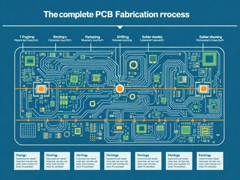
3. How the Printed Circuit Board Soldering Process Works: Step by Step
A professional printed circuit board soldering process begins before the board enters the assembly line. PCB design, component selection, solder paste specifications, stencil design, and surface finish all influence the final joint quality.
Step 1: PCB Design and Manufacturing Preparation
Before assembly, the manufacturer reviews PCB Gerber files, drill data, bill of materials (BOM), component footprints, and assembly drawings.
The engineering team checks pad dimensions, component spacing, solder mask openings, thermal reliefs, and assembly clearances. Poor pad design can cause tombstoning, solder bridging, insufficient wetting, and other defects.
For complex boards, we recommend a design-for-manufacturability (DFM) review before production. This is particularly important for fine-pitch components, BGA packages, HDI boards, and multilayer PCB structures.
When the board design requires complex layer construction, review the manufacturing feasibility of sequential lamination PCB structures early in the engineering process.
Step 2: Solder Paste Printing
For SMT assembly, solder paste is deposited onto PCB pads through a stainless-steel stencil. The paste generally contains fine solder alloy particles suspended in a flux medium.
A solder paste printer aligns the stencil with the PCB and controls the printing operation. The objective is to deposit a consistent amount of paste at the correct locations.
Important variables include:
Stencil thickness and aperture geometry.
Stencil-to-board alignment.
Squeegee pressure and printing speed.
Solder paste storage and working temperature.
Paste release and transfer efficiency.
PCB cleanliness and flatness.
Too much solder paste can cause bridges between adjacent pads. Too little can result in insufficient solder volume or open connections. For fine-pitch components, stencil design deserves particular attention.
Step 3: Component Placement
Automated pick-and-place equipment positions components onto the solder paste deposits. Machine vision systems verify component orientation and placement coordinates.
Placement accuracy becomes increasingly important as component sizes decrease and pin spacing becomes tighter.
For commercial users, automated placement offers much better repeatability than relying on manual positioning for large production volumes. However, machine calibration, feeder condition, component packaging, and board support must also be controlled.
Step 4: Reflow Soldering
The populated PCB enters a reflow oven, where controlled heating melts the solder paste and creates the solder joints.
A typical reflow profile includes four functional stages:
Preheating: Raises the PCB temperature gradually and reduces excessive thermal shock.
Soaking: Allows temperature equalization and supports flux activation.
Reflow: Raises the solder above its liquidus temperature so the alloy melts and forms joints.
Cooling: Solidifies the solder and establishes the final joint structure.
Reflow temperature and timing depend on the solder alloy, component specifications, board thermal mass, and paste manufacturer's recommendations. A profile should be verified through actual temperature measurements rather than copied from another product.
Step 5: Through-Hole Soldering Where Required
Boards containing through-hole components require an additional soldering operation when those connections are not made manually or through another qualified process.
Wave soldering passes the PCB over a controlled wave of molten solder. Selective soldering uses a localized solder nozzle to connect specific through-hole pins.
The decision depends on board geometry, component placement, thermal sensitivity, and production requirements.
Step 6: Cooling and Post-Solder Cleaning
After soldering, the PCB must cool under appropriate conditions. Excessive mechanical handling while solder joints are still hot can disturb the connections.
Flux residues may remain after soldering. Whether cleaning is required depends on the flux chemistry, assembly requirements, and intended operating environment. No-clean flux does not mean that every residue is harmless under every application condition.
For high-reliability or contamination-sensitive assemblies, define cleanliness requirements and verify them using an appropriate test method.
Step 7: Inspection and Electrical Testing
After soldering, the assembly is inspected for visible and hidden defects. Depending on the product, the manufacturer may use AOI, X-ray inspection, visual inspection, continuity testing, and functional testing.
Inspection should be selected according to the actual component package and failure risk. A visually acceptable joint does not automatically prove long-term reliability.
4. Main Types of PCB Soldering Processes
4.1 Reflow Soldering: Best for Modern SMT PCB Assembly
Reflow soldering is the standard approach for most surface-mount PCB assembly operations. Solder paste is printed onto PCB pads, components are placed, and the complete assembly passes through a controlled heating cycle.
It is particularly suitable for small components, fine-pitch integrated circuits, and high-density electronic designs.
Benefits:
Compatible with automated high-speed SMT lines.
Supports compact and high-density PCB layouts.
Provides consistent process control when properly validated.
Suitable for a wide range of SMT packages, including BGA.
Supports repeatable prototype and mass-production workflows.
Limitations: Reflow soldering requires accurate stencil printing, placement, and thermal profiling. Excessive heat or incorrect process settings can damage components or produce poor joints.
Our recommendation is to use reflow soldering for SMT-heavy products rather than trying to substitute manual soldering for a process designed for automation.
4.2 Wave Soldering: Best for Suitable Through-Hole Assemblies
Wave soldering uses a controlled wave of molten solder to connect through-hole component leads to PCB pads and plated holes. The board typically passes through flux application and preheating before contacting the solder wave.
This method is well suited to production boards containing conventional through-hole components, particularly when the layout allows solder to reach the required connections.
Benefits: High production efficiency, repeatable soldering, and suitability for compatible through-hole assemblies.
Limitations: Dense SMT layouts, heat-sensitive components, and unsuitable board geometries can make wave soldering difficult. Solder bridging and shadowing must also be managed.
4.3 Selective Soldering: Best for Mixed-Technology PCB Assemblies
Selective soldering applies molten solder to specific through-hole connections rather than exposing an entire board edge or surface to a solder wave.
It is particularly useful when a PCB combines SMT components with connectors, terminals, or other through-hole parts that cannot be conveniently wave soldered.
Benefits:
Localized heating reduces exposure of surrounding components.
Supports complex mixed-technology PCB layouts.
Can reduce manual soldering requirements.
Provides repeatable connections when properly programmed.
Limitations: Equipment programming, nozzle selection, board fixturing, and process setup can increase initial costs. For very simple low-volume boards, it may not be economical.
4.4 Hand Soldering: Best for Prototypes and Repair
Hand soldering uses a soldering iron to heat a specific component lead and PCB pad. It remains useful for engineering prototypes, component replacement, repair, and limited production work.
However, manual soldering introduces greater dependence on operator technique, temperature control, and inspection discipline.
For beginners, hand soldering is a practical learning and repair method. For high-volume commercial production, automated methods generally provide better consistency and productivity.
4.5 Laser Soldering: A Specialized Precision Option
Laser soldering uses a focused laser beam to heat a localized solder joint. It can be useful when conventional heating methods expose nearby components or materials to excessive thermal stress.
It is worth considering for specialized assemblies with demanding access, precision, or thermal requirements. However, laser soldering equipment and process development may not be justified for ordinary PCB assembly.
5. PCB Soldering Materials: Solder Alloys, Flux, and PCB Surface Finishes
The printed circuit board soldering process depends on more than equipment. Solder alloy, flux chemistry, PCB surface finish, component metallization, and storage conditions all influence joint quality.
5.1 Lead-Free Solder vs Leaded Solder
Lead-free solder is widely used in modern electronics manufacturing to meet applicable environmental and market requirements. Common lead-free formulations include SAC alloys, such as SAC305, which contain tin, silver, and copper.
Traditional SnPb solder alloys have lower melting temperatures than common SAC lead-free alloys and may still be specified in certain applications where permitted.
| Factor | Lead-Free Solder | Leaded Solder |
|---|---|---|
| Common example | SAC305 | Sn63/Pb37 |
| Typical melting behavior | Higher melting range; SAC305 liquidus approximately 217°C | Eutectic melting point approximately 183°C |
| Environmental considerations | Used to meet applicable lead-restriction requirements | Subject to restrictions and exemptions in relevant markets |
| Thermal process | Generally requires higher reflow temperatures | Generally requires lower reflow temperatures |
| Selection considerations | RoHS compliance, reliability, component limits, and alloy performance | Specific permitted applications and established process requirements |
We recommend selecting solder alloy based on the product's regulatory requirements, operating environment, component compatibility, and validated manufacturing process. Do not assume that lead-free solder is automatically superior in every technical application or that leaded solder can be used without checking applicable restrictions.
5.2 Why Flux Matters
Flux helps remove or disrupt oxide layers and improves solder wetting. It also influences residue characteristics, cleaning requirements, and process stability.
Common flux categories include rosin-based, water-soluble, and no-clean formulations. Each has different handling and post-solder requirements.
For production assembly, use a flux system compatible with the solder paste or wire alloy, PCB surface finish, and cleaning process.
5.3 How PCB Surface Finish Affects Soldering
PCB surface finish protects exposed copper and provides a solderable surface for component attachment. The choice can affect shelf life, solderability, cost, and suitability for fine-pitch designs.
| PCB Surface Finish | Key Characteristics | Suitable Applications | Purchasing Advice |
|---|---|---|---|
| HASL / Lead-Free HASL | Solder-coated copper surface; economical and widely used | General-purpose electronics | Good value when pad flatness requirements are moderate |
| OSP | Organic protective coating over copper | Cost-sensitive SMT applications | Manage storage and assembly exposure carefully |
| Immersion Silver | Flat solderable surface | Fine-pitch and selected high-performance boards | Pay attention to packaging and tarnish prevention |
| Immersion Tin | Flat tin surface with good solderability when properly handled | SMT and selected fine-pitch applications | Control storage and handling conditions |
| Hard Gold | Durable gold finish, often used for contact surfaces | Edge contacts and wear-resistant electrical interfaces | Do not automatically specify it for ordinary solder pads |
For most ordinary SMT applications, the best surface finish is the one that meets the board's solderability, flatness, storage, and cost requirements. More expensive finishes are not automatically better for every design.
6. Important Parameters That Determine PCB Soldering Quality
Even high-quality solder paste and advanced equipment cannot compensate for uncontrolled process parameters. Professional assembly manufacturers validate the complete soldering process rather than relying on a single machine setting.
Temperature Profile
The temperature profile determines how the PCB and components experience heating, melting, and cooling. The correct profile depends on solder alloy, board thickness, component thermal mass, and manufacturer recommendations.
Time Above Liquidus
Time above liquidus (TAL) is the period during which the solder temperature remains above the alloy's liquidus temperature. Insufficient time can lead to incomplete melting or poor wetting, while excessive exposure can increase oxidation and thermal damage risks.
Solder Paste Volume
Solder paste volume influences joint formation. Incorrect stencil thickness, aperture design, or printing conditions can result in insufficient solder, excessive solder, bridging, and tombstoning.
Component Placement Accuracy
Incorrect component placement can create alignment problems and uneven solder connections. Fine-pitch packages and small passive components are particularly sensitive to placement and paste consistency.
Cooling Rate
Cooling influences solidification and the resulting joint structure. A suitable cooling profile should follow alloy and assembly process requirements while avoiding unnecessary thermal stress.
7. Pros and Cons of Different PCB Soldering Processes
| Method | Advantages | Disadvantages | Our Verdict |
|---|---|---|---|
| Reflow soldering | High automation, excellent SMT compatibility, repeatable production | Requires accurate printing and thermal profile control | Best general-purpose method for SMT assembly |
| Wave soldering | Efficient for suitable through-hole production | Limited flexibility for dense mixed-technology boards | Good for compatible through-hole production |
| Selective soldering | Localized heating and good control of specific joints | Higher setup and programming requirements | Worth using for complex mixed-technology designs |
| Hand soldering | Flexible and inexpensive for small jobs | Operator-dependent and less scalable | Best for prototypes and repair |
| Laser soldering | Precise localized heating | Higher equipment and process-development costs | Use only when specialized requirements justify it |
The key commercial consideration is total production cost, not equipment price alone. A process that reduces rework and improves repeatability may be more economical over the full production lifecycle.
8. Reflow vs Wave vs Selective Soldering: Which Is Better?
These three methods are often compared when manufacturers select a PCB assembly partner. The correct choice depends primarily on the component mounting technology and board layout.
| Comparison Factor | Reflow | Wave | Selective |
|---|---|---|---|
| Primary component type | SMT | Through-hole | Through-hole |
| Heating method | Controlled oven heating | Molten solder wave | Localized molten solder |
| Fine-pitch SMT compatibility | Excellent | Limited | Not its primary purpose |
| Mixed-technology compatibility | Requires complementary soldering where needed | Depends on board layout and component protection | Very good for selected through-hole joints |
| Production automation | High | High | High |
| Setup complexity | Moderate to high | Moderate | Moderate to high |
| Best production scenario | SMT-heavy electronic products | Suitable through-hole production | Complex mixed-technology boards |
Which Process Should Beginners Choose?
For beginners developing an ordinary SMT product, reflow soldering through a professional assembly provider is generally the most practical option. It offers a scalable production route and supports modern component packages.
Which Process Should Commercial Manufacturers Choose?
For commercial manufacturers, the choice should follow the BOM and assembly drawings. A board with SMT components and several through-hole connectors may need reflow followed by selective soldering. A simpler through-hole product may be more economical with wave soldering.
We do not recommend forcing every PCB into a single soldering process simply to reduce setup costs. The wrong method can increase rework and compromise product quality.
9. Common PCB Soldering Defects and How to Prevent Them
Soldering defects are not all caused by incorrect temperatures. Some originate from PCB design, material handling, stencil printing, component placement, or surface contamination.
| Defect | Common Causes | Practical Prevention |
|---|---|---|
| Solder bridge | Excessive paste, poor pad spacing, misalignment | Optimize stencil apertures and placement accuracy |
| Cold or disturbed joint | Insufficient heating, movement during solidification, poor wetting | Validate the thermal process and handling |
| Tombstoning | Uneven heating or unbalanced solder forces | Review pad geometry, thermal balance, and paste deposits |
| Insufficient solder | Low paste volume or poor printing transfer | Inspect stencil and printing conditions |
| Voiding | Flux outgassing, paste chemistry, process conditions | Optimize materials and thermal profile |
| Non-wetting | Oxidation, contamination, unsuitable surface condition | Verify material quality and surface finish |
| Component damage | Excessive thermal exposure or poor handling | Respect component thermal limits and handling requirements |
| Head-in-pillow defect | Package warpage, paste or reflow issues | Control package coplanarity, paste deposition, and reflow conditions |
Why Soldering Defects Should Be Investigated at Their Source
Repeatedly repairing defective boards without identifying the underlying cause is an expensive production strategy. If solder bridges appear across multiple batches, the engineering team should review stencil apertures, paste printing, component alignment, and board design.
Similarly, recurring BGA defects may require X-ray inspection and a review of package coplanarity, solder paste volume, and thermal profile conditions.
For professional manufacturers, a structured root-cause process is more valuable than simply increasing the number of repaired boards.
10. PCB Soldering Inspection and Quality Control
Inspection verifies whether the soldering process has produced acceptable joints. The inspection strategy should combine appropriate visual, automated, and electrical verification methods.
10.1 Visual Inspection
Visual inspection can identify obvious problems such as missing components, contamination, incorrect orientation, solder bridges, and visible joint abnormalities.
It remains useful for prototypes and production sampling, but it cannot reliably identify every hidden solder defect.
10.2 Automated Optical Inspection (AOI)
AOI uses cameras and image-processing systems to inspect PCB assemblies. It can detect component presence, polarity, alignment, and many visible soldering defects.
For commercial SMT assembly, AOI is a valuable production control because it supports consistent inspection and faster feedback to the assembly line.
See our PCB AOI inspection service for more information about automated optical inspection.
10.3 X-Ray Inspection
X-ray inspection is particularly important for solder joints hidden underneath BGA, QFN, and other bottom-terminated packages. It can reveal voiding, bridging, missing connections, and certain structural abnormalities that cannot be seen from the board surface.
However, X-ray results must be interpreted against appropriate acceptance criteria. A particular void percentage or visual appearance should not automatically be treated as a universal pass or fail condition.
For dense electronic assemblies, our recommendation is to use PCB X-ray inspection when the component package and product risk justify it.
10.4 Electrical Testing
Electrical testing checks whether the PCB meets defined electrical requirements. Depending on the design, this may include continuity, isolation, short-circuit detection, and functional verification.
Explore our PCB electrical testing service for additional information.
10.5 IPC Workmanship Standards
IPC-A-610 provides acceptance criteria for electronic assemblies, while IPC J-STD-001 addresses requirements for soldered electrical and electronic assemblies. These standards are commonly referenced in professional electronics manufacturing.
The appropriate class, revision, and contractual acceptance requirements should be agreed upon before production. Passing an inspection standard does not independently guarantee a particular service life or field failure rate.
11. How to Choose a Reliable PCB Assembly Manufacturer
A reliable soldering process depends heavily on the manufacturing partner. Buyers should evaluate the supplier's engineering capability, SMT equipment, process controls, inspection coverage, and production experience rather than selecting solely on quotation price.
Check SMT Production Capabilities
Ask whether the manufacturer supports the component sizes, fine-pitch ICs, BGA packages, and board dimensions required by your design.
For high-density electronic assemblies, verify that the supplier has suitable stencil printing, automated placement, reflow profiling, and inspection capabilities.
Evaluate Process Control
Ask how the supplier validates soldering profiles, manages solder paste, monitors equipment calibration, and handles production deviations.
A capable manufacturer should be able to explain how process parameters are controlled and what records are available for quality investigations.
Review Quality Inspection Capabilities
Check whether the manufacturer provides AOI, X-ray inspection, electrical testing, and functional testing where required.
Do not assume that every assembly requires every inspection method. A good supplier should explain why a particular method is appropriate for your design.
Confirm Prototype and Mass Production Support
For new products, prototype assembly is useful for validating component placement, solderability, and initial functional performance. However, a successful prototype does not automatically prove that mass production will be equally reliable.
Look for a manufacturer capable of maintaining process consistency as volumes increase. Compare quick-turn PCB production with high-volume PCB manufacturing according to your actual production schedule.
Check Engineering and Design Support
A strong assembly partner should identify manufacturing problems before they become production defects. Ask whether the supplier can review Gerber files, BOM data, component footprints, and assembly drawings.
For complex designs, PCB design support services can reduce the risk of avoidable assembly problems.
12. PCB Soldering Costs: What Determines the Price?
The cost of the printed circuit board soldering process depends on board complexity, component count, assembly technology, production volume, inspection requirements, and material selection.
A low-cost assembly quotation may be attractive, but buyers should compare the complete production scope. A supplier that excludes necessary inspection or has limited process controls may create higher downstream costs.
Main Factors Affecting PCB Soldering Costs
Component count: More components generally increase placement and inspection time.
Component package complexity: Fine-pitch ICs and BGA packages require more demanding assembly and inspection.
PCB dimensions and layers: Board size, thermal mass, and multilayer construction can influence processing requirements.
Stencil and tooling: SMT stencil production and specialized fixtures add setup costs.
Soldering method: Reflow, wave, and selective soldering have different equipment and process costs.
Material selection: Solder alloys and PCB surface finishes affect procurement and processing costs.
Inspection requirements: AOI, X-ray, and functional testing add cost but may reduce the risk of undetected defects.
Production volume: Setup costs are distributed differently across prototype, small-batch, and mass production.
Is It Worth Paying More for Advanced PCB Assembly?
For simple, low-risk electronic products, an unnecessarily complex inspection and soldering package may not be commercially justified.
For industrial control boards, automotive electronics, medical products, and other demanding applications, more extensive process validation and inspection can be worth the additional cost.
For example, a BGA assembly with hidden solder joints may justify X-ray inspection. A simple board without hidden connections may obtain sufficient inspection coverage through AOI and electrical testing, depending on its requirements.
Our recommendation is to calculate total cost rather than focus on the lowest assembly price. Consider material losses, rework, warranty exposure, production delays, and the cost of field failures.
13. 365PCB Expert Recommendations for Reliable PCB Soldering
At 365PCB, we believe the most reliable printed circuit board soldering process starts with matching the manufacturing method to the product's technical requirements.
For SMT-heavy designs, we recommend automated SMT assembly with controlled solder paste printing, accurate component placement, and validated reflow profiles. This is generally the most practical route for modern electronic products that require consistent assembly quality.
For mixed-technology boards, determine whether through-hole components are better handled through wave soldering, selective soldering, or a controlled manual operation. Do not select a method solely because it is already available on the production line.
365PCB SMT PCB Assembly Services
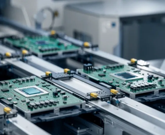
365PCB provides professional SMT PCB assembly services using advanced automated SMT production lines. The service supports prototype development through volume production, with no minimum order quantity stated for its SMT offering.
Our SMT assembly capabilities support:
0402 chip components and fine-pitch integrated circuits.
BGA and other complex surface-mount packages.
Automated high-speed component placement.
Lead-free RoHS and leaded soldering options, subject to applicable requirements.
Quality inspection and assembly process control.
Prototype and production-volume PCB assembly.
For buyers developing new electronics, choosing an assembly provider with both technical support and scalable production capabilities can simplify the transition from prototype to commercial manufacturing.
Explore 365PCB SMT PCB Assembly ServicesWhich Industries Benefit from Professional PCB Soldering?
Different industries have different assembly priorities. The soldering process should be selected according to the product's operating environment and reliability requirements.
Consumer electronics: Prioritize repeatable SMT assembly, compact layouts, and production efficiency. See our consumer electronics PCB solutions.
Automotive electronics: Emphasize process traceability, thermal performance, and application-specific qualification. Explore automotive PCB manufacturing.
Medical electronics: Require clearly documented quality controls and product-specific verification. Review our medical PCB solutions.
Industrial control systems: Focus on durable connections, environmental requirements, and long-term production consistency. See our industrial control PCB solutions.
Our Final Buying Advice
Before choosing a PCB assembly manufacturer, provide the supplier with the Gerber files, BOM, assembly drawings, required solder alloy, surface finish requirements, and expected production volume.
Ask the supplier to explain its recommended soldering method and inspection plan. A capable manufacturer should be able to justify its recommendations based on the actual PCB design rather than offering the same process for every customer.
Reliable soldering is not achieved by buying the most expensive equipment or selecting the highest-cost solder alloy. It comes from a controlled process, suitable materials, sound engineering, and consistent verification.
14. Frequently Asked Questions About the Printed Circuit Board Soldering Process
1. What are the main steps in the printed circuit board soldering process?
The main steps include PCB preparation, solder paste printing for SMT assembly, component placement, reflow soldering, through-hole soldering where required, cooling, cleaning when necessary, inspection, and electrical testing. The exact workflow depends on the board design and component technology.
2. What is the most common PCB soldering method?
Reflow soldering is the most common method for modern SMT PCB assembly. It is suitable for surface-mount components, including small passive devices, fine-pitch integrated circuits, and BGA packages. Through-hole components may require wave or selective soldering.
3. What is the difference between reflow soldering and wave soldering?
Reflow soldering melts solder paste deposited on PCB pads to connect surface-mount components. Wave soldering uses a wave of molten solder to connect suitable through-hole component leads. The two methods serve different assembly requirements.
4. What temperature is used in PCB soldering?
The required temperature depends on the solder alloy and process. For example, SAC305 lead-free solder has a liquidus temperature of approximately 217°C, while eutectic Sn63/Pb37 solder melts at approximately 183°C. Actual reflow oven settings and peak component temperatures must be established through process profiling and material specifications.
5. Is lead-free solder better than leaded solder?
Lead-free solder is widely used to meet applicable environmental regulations, including RoHS requirements. However, it generally requires higher processing temperatures than traditional SnPb solder. The best choice depends on regulatory obligations, product requirements, component limitations, and manufacturing qualification.
6. What causes poor solder joints on a PCB?
Common causes include insufficient solder paste, poor wetting, oxidation, contamination, incorrect thermal profiles, component misalignment, and unsuitable PCB pad design. Manufacturers should investigate the underlying process rather than relying exclusively on rework.
7. How can manufacturers inspect PCB soldering quality?
Manufacturers can use visual inspection, automated optical inspection (AOI), X-ray inspection, electrical testing, and functional testing. The appropriate method depends on the component packages, hidden connections, product risks, and contractual acceptance criteria.
8. What is the best PCB surface finish for soldering?
There is no universally best surface finish. HASL, lead-free HASL, OSP, immersion silver, and immersion tin are commonly selected according to solderability, pad flatness, storage conditions, component pitch, and cost. The correct choice should match the PCB design and assembly process.
9. Can SMT PCB assembly support prototype orders?
Yes. SMT PCB assembly can support prototype, small-batch, and mass-production requirements. Prototype assembly helps validate component placement, soldering performance, and functionality before commercial production. 365PCB offers SMT assembly services with no minimum order quantity stated for its service.
10. How do I choose a reliable PCB soldering manufacturer?
Evaluate SMT equipment, soldering process controls, component compatibility, reflow profiling, AOI and X-ray capabilities, electrical testing, engineering support, and production scalability. Ask for a process recommendation based on your actual PCB design and quality requirements.
15. Technical References and Industry Standards
The following authoritative resources are useful when establishing PCB soldering processes, acceptance criteria, and manufacturing quality requirements.
IPC – Association Connecting Electronics Industries. Industry standards and technical resources covering PCB design, electronic assembly, soldering workmanship, and acceptance criteria. Relevant documents include IPC-A-610 and IPC J-STD-001.
ISO 9001 – Quality Management Systems. International quality management requirements relevant to manufacturing process control, documented procedures, and continual improvement.
European Commission – RoHS Directive. Official information concerning restrictions on hazardous substances in electrical and electronic equipment, including lead-related requirements and applicable exemptions.
Important: Always verify the current revisions of applicable standards, customer specifications, and regulatory requirements before establishing soldering acceptance criteria.