English
Microelectronics manufacturing is no longer just a matter of putting electronic components onto a circuit board. OEMs are dealing with increasingly compact designs, high-density interconnections, sensitive semiconductor devices, tighter thermal limits, more demanding reliability requirements, and supply chains that can make or break a product launch. A design that looks excellent in an engineering file can still become expensive or unreliable when it reaches manufacturing.
For OEMs, the practical challenge is knowing which manufacturing capabilities matter, where quality risks occur, and how to choose suppliers that can support a product from prototype through repeat production. The right decision is not always the supplier offering the lowest unit price. It is the supplier whose process capabilities match the product's technical requirements and commercial goals.
Quick Answer: What Should OEMs Know About Microelectronics Manufacturing?
OEMs should evaluate microelectronics manufacturing across the complete product chain: semiconductor devices, packaging and interconnection, PCB design and fabrication, electronic assembly, inspection, testing, and supply-chain control. The most important decisions are made early: select a manufacturable architecture, specify materials and tolerances, confirm supplier capabilities, define inspection and test requirements, and validate the production process before committing to large orders.
Our recommendation: Choose manufacturing partners based on demonstrated technical capability, process control, engineering communication, and production consistency—not on a price quotation alone. For products built around complex PCBs, HDI structures, fine-pitch ICs, or BGA components, involve the fabricator and assembly provider before the design is frozen.
What Is Microelectronics Manufacturing?
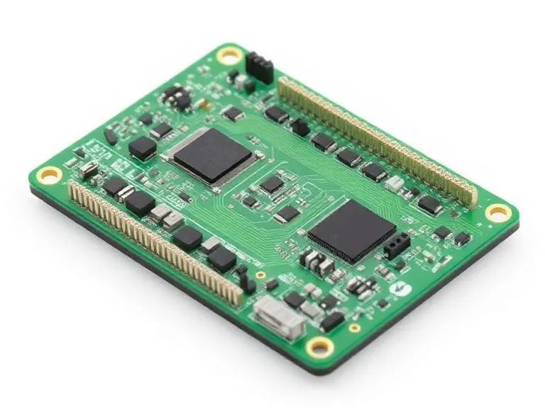
Microelectronics manufacturing is the set of technologies and production processes used to create, package, interconnect, and assemble miniaturized electronic systems. It includes semiconductor device fabrication, advanced chip packaging, substrate manufacturing, printed circuit board fabrication, and electronic assembly.
These activities are related, but they are not interchangeable. Semiconductor wafer fabrication creates the integrated circuits themselves. Packaging connects and protects semiconductor dies. PCB fabrication produces the circuit boards that connect electronic components. PCBA manufacturing mounts and solders components onto those boards to create functional electronic assemblies.
For many OEMs, the commercial requirement is not to manufacture silicon wafers in-house. It is to source suitable semiconductor devices and work with capable suppliers to produce the substrates, circuit boards, and assemblies that turn those devices into a reliable product.
Microelectronics Manufacturing vs. PCB Manufacturing
PCB manufacturing is one important part of the broader microelectronics ecosystem. A conventional PCB provides electrical and mechanical connections between components. A high-density PCB may use smaller features, finer spacing, microvias, sequential lamination, and more complex interconnection structures.
Advanced microelectronics may also involve chiplets, system-in-package (SiP), IC substrates, flexible circuits, and heterogeneous integration. These technologies place greater demands on dimensional accuracy, electrical performance, thermal management, and inspection.
OEMs should therefore define the actual manufacturing scope before requesting quotations. A supplier that specializes in standard PCB fabrication may not have the capabilities required for advanced semiconductor packaging. Likewise, a semiconductor packaging specialist may not be the right partner for complete SMT PCB assembly.
How Does the Microelectronics Manufacturing Process Work?
The exact process depends on the product architecture. A semiconductor device, an HDI circuit board, and a finished SMT assembly have different production routes. However, OEM projects commonly pass through a sequence of design, material selection, fabrication, assembly, inspection, and validation stages.
1. Product Architecture and Engineering Design
Manufacturing begins with the electrical and mechanical requirements. Engineers define the circuit architecture, component selection, board dimensions, interconnection strategy, operating temperature, power requirements, and expected service life.
At this stage, OEMs should consider design for manufacturability (DFM) and design for assembly (DFA). Component spacing, package selection, thermal paths, test access, and board stack-up can affect production cost and yield. A design that ignores these factors may require expensive revisions later.
For projects requiring layout review or engineering input, PCB design support services can help address fabrication constraints before the manufacturing release.
2. Material and Component Selection
Material selection affects electrical performance, mechanical stability, heat resistance, and long-term reliability. Depending on the application, an OEM may need standard FR-4, high-Tg laminate, low-loss RF material, flexible substrates, or specialized materials for high-density interconnection.
Component selection is equally important. Semiconductor package type, pitch, power dissipation, availability, and lifecycle status should all be considered. A component that performs well electrically may still create sourcing or assembly problems if it is difficult to procure or requires specialized handling.
For OEMs, the best approach is to approve critical materials and components before the design enters production. Late substitutions should be evaluated by engineering rather than accepted as purchasing decisions.
3. PCB Fabrication and Substrate Production
PCB fabrication converts the approved design data into a physical circuit board. Depending on the construction, this can involve imaging, etching, drilling, plating, lamination, solder-mask application, surface finishing, routing, and electrical testing.
Complex designs may require multilayer lamination, laser-drilled microvias, blind and buried vias, controlled impedance, or sequential build-up processes. These requirements should be confirmed with the fabricator before the design is finalized.
OEMs should not assume that every PCB supplier can produce every stack-up. Confirm the supplier's actual layer-count range, material experience, minimum feature capability, via structures, thickness tolerances, and inspection process.
4. SMT PCB Assembly and Component Placement
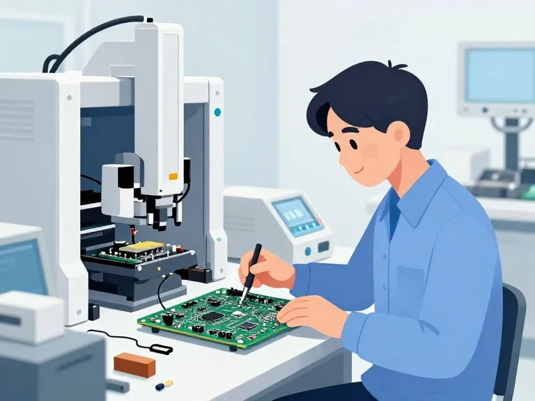
After fabrication, components are mounted onto the PCB. Surface Mount Technology (SMT) is widely used because it supports automated, high-speed placement of compact components. A typical SMT process includes solder paste printing, component placement, reflow soldering, and post-assembly inspection.
Fine-pitch ICs, 0402 components, QFNs, and BGAs require careful control of solder paste, placement accuracy, thermal profiles, and component handling. A defect that is easy to see on a large connector may be hidden beneath a BGA package.
365PCB provides SMT PCB assembly services using automated SMT lines for prototype and volume production, supporting fine-pitch ICs and BGA packages. The service scope includes lead-free and leaded soldering options and inspection aligned with applicable IPC requirements. OEMs should confirm the exact process, acceptance criteria, and inspection coverage required for each project.
5. Inspection, Electrical Testing, and Functional Validation
Inspection verifies that the board and assembly conform to the approved requirements. Depending on the design, this may include automated optical inspection (AOI), X-ray inspection, electrical continuity testing, insulation testing, in-circuit testing, and functional testing.
Inspection methods should be selected according to the risks they are intended to detect. AOI is useful for visible placement and soldering issues, while X-ray inspection can reveal certain hidden solder-joint defects. Electrical testing checks for opens and shorts, and functional testing confirms that the assembly operates as intended.
No single inspection method proves total product reliability. A strong quality plan combines suitable inspection coverage with process controls, traceability, and validation testing.
Key Microelectronics Manufacturing Technologies OEMs Should Understand
Not every product needs advanced packaging or ultra-high-density PCB technology. OEMs should select technology based on electrical performance, size, reliability, production volume, and total cost. Specifying more advanced technology than the product needs can increase manufacturing cost without delivering a meaningful commercial benefit.
High-Density Interconnect (HDI) PCB
HDI PCBs use finer lines and spaces, smaller vias, and higher-density interconnections than conventional PCB constructions. They are useful when an OEM needs to reduce board size, route complex circuitry, or accommodate dense component layouts.
HDI is worth considering for compact communication devices, portable electronics, high-density computing modules, and designs using fine-pitch components. However, it adds process complexity. OEMs should review stack-up design, microvia reliability, registration, and supplier experience before choosing an HDI structure.
Flexible and Rigid-Flex Circuits
Flexible PCBs allow circuits to bend or fit into irregular spaces. Rigid-flex designs combine rigid board sections with flexible interconnections. They can reduce connectors and cable assemblies while improving packaging flexibility.
These technologies are particularly useful in compact medical equipment, wearable devices, cameras, industrial sensors, and products with moving or constrained mechanical assemblies. They are not automatically better than conventional rigid PCBs. Bend radius, copper design, stiffener placement, and mechanical life must be evaluated carefully.
See flexible PCB manufacturing for applications where space, movement, and mechanical integration are important design factors.
System-in-Package (SiP)
System-in-Package technology integrates multiple semiconductor dies or components within one package. It can combine different functions in a compact footprint and reduce the need for separate board-level components.
SiP is relevant when an OEM needs compact integration, performance optimization, or a combination of technologies that would be difficult to implement using a single monolithic chip. The trade-offs include more complex package design, thermal management, test access, and supplier qualification.
Explore SiP PCB-related manufacturing when evaluating circuit-board requirements associated with system-in-package products. Confirm whether the supplier's scope covers the PCB, substrate, package, or assembly stage you actually need.
IC Substrates and Semiconductor Test Boards
IC substrates provide dense electrical connections between semiconductor dies and external circuitry. Their dimensional and electrical requirements can be substantially different from those of standard PCBs.
Semiconductor test boards are used in test environments to connect devices under test with automated test equipment. Probe cards, load boards, and other test interfaces must meet demanding requirements for signal integrity, contact reliability, and mechanical accuracy.
For projects in this area, review the specific capabilities required for IC substrate PCB, probe card PCB, and load board PCB applications. These are specialized products, so supplier selection should be based on relevant process experience rather than general PCB production claims.
Benefits and Limitations of Advanced Microelectronics Manufacturing for OEMs
Advanced manufacturing can make products smaller, faster, more power-efficient, and more integrated. But those gains are not free. The OEM must balance performance improvements against design complexity, supplier capability, inspection requirements, and production economics.
Main Benefits
Higher functional density: HDI, fine-pitch components, and advanced packaging allow more functionality in less physical space.
Improved product integration: SiP and advanced interconnection technologies can reduce separate components and simplify some system architectures.
Better electrical performance: Appropriate materials, stack-up design, and controlled impedance can support high-speed and RF applications.
More flexible product design: Flexible and rigid-flex circuits help engineers fit electronics into compact or moving assemblies.
Scalable manufacturing: Automated PCB assembly can provide repeatable component placement and support higher production volumes.
Potential cost reduction at scale: A well-designed product can reduce assembly steps, material waste, and unit cost as production volume increases.
Limitations OEMs Must Plan For
Higher initial engineering cost: Advanced stack-ups, substrates, test fixtures, and process validation may increase upfront investment.
More demanding quality controls: Dense designs can make inspection and rework more difficult.
Supplier dependency: Specialized materials and processes may limit the number of qualified manufacturing partners.
Supply-chain exposure: Advanced semiconductor components can have long lead times or limited sourcing options.
Thermal and reliability challenges: Higher power density and compact packaging can make heat dissipation more difficult.
| Advantages | Limitations |
|---|---|
| More functionality in compact product designs. | Greater layout, fabrication, and assembly complexity. |
| Potentially improved signal integrity and electrical performance. | Material selection and process control become more demanding. |
| Automated assembly supports repeatability and scale. | Equipment, programming, and test requirements can increase setup costs. |
| Integration may reduce connectors and separate assemblies. | Repair, inspection, and redesign can become more difficult. |
| Advanced packaging can improve system-level performance. | Specialized suppliers and qualification may be required. |
Microelectronics Manufacturing Technologies: Comparison for OEM Decisions
The following comparison is a practical starting point. Actual suitability depends on the design, operating environment, and the capabilities of the selected supplier.
| Technology | Primary Purpose | Best-Fit Applications | Main OEM Consideration |
|---|---|---|---|
| Standard multilayer PCB | Connects components across multiple copper layers. | Industrial controls, consumer electronics, embedded systems. | Balance layer count, stack-up, material, and routing needs. |
| HDI PCB | Supports dense routing and compact component placement. | Mobile devices, compact computing, advanced communication equipment. | Validate microvia design, registration, and supplier capability. |
| Flexible PCB | Provides bendable electrical interconnections. | Wearables, cameras, medical devices, compact assemblies. | Check bend radius, copper construction, and mechanical life. |
| Rigid-flex PCB | Combines rigid and flexible circuit sections. | Space-constrained systems and products with moving sections. | Review transition zones, stack-up, and assembly handling. |
| SiP | Integrates multiple dies or components in one package. | Compact modules, RF systems, high-integration electronics. | Assess thermal, test, package, and integration complexity. |
| IC substrate | Connects semiconductor dies to package-level interconnections. | Advanced semiconductor packaging. | Requires specialized substrate capabilities and inspection. |
| SMT PCB assembly | Mounts electronic components onto fabricated PCBs. | Most modern electronic products and control boards. | Check placement capability, soldering process, and test coverage. |
For most OEMs developing a conventional electronic product, the practical starting point is a well-designed PCB with a suitable SMT assembly process. Advanced packaging or HDI should be selected when the product's size, performance, or integration requirements justify the added cost—not simply because the technology sounds more advanced.
Microelectronics Manufacturing Applications: Which Technologies Fit Which Products?
Industrial Electronics and Automation
Industrial control systems, sensors, motor drives, and monitoring equipment often need stable operation across temperature changes, electrical noise, and long service periods. OEMs should prioritize component lifecycle, thermal design, PCB material suitability, and repeatable assembly quality.
For these products, a conventional multilayer PCB may be entirely sufficient. Use HDI only when component density or physical size makes it necessary. For long-life equipment, material availability and change control can be more important than achieving the smallest possible board.
Medical and Diagnostic Equipment
Medical electronics can involve compact signal-processing circuits, sensor interfaces, power-management electronics, and flexible interconnections. Product requirements vary significantly according to intended use and regulatory classification.
OEMs should define traceability, supplier qualification, documentation, and verification requirements early. Do not assume that a supplier's general quality certification automatically establishes compliance for a specific medical product. The OEM remains responsible for defining and verifying applicable regulatory and quality obligations.
Telecommunications and RF Equipment
RF and high-speed communication products require careful control of impedance, dielectric properties, loss, grounding, and interconnection geometry. Material selection and stack-up design can have a direct effect on electrical performance.
For these applications, involve the PCB fabricator during design review. A material substitution that appears commercially convenient may change insertion loss, dielectric behavior, or other performance characteristics.
Automotive and Transportation Electronics
Automotive electronics can face vibration, thermal cycling, humidity, electrical transients, and long product lifecycles. OEMs should specify the relevant component qualification, assembly requirements, test strategy, and traceability expectations for the application.
For safety-related or mission-critical systems, supplier selection should include evidence of process discipline and change management. A low-cost board that cannot maintain consistent quality is not a commercial saving.
Semiconductor Test and Advanced Computing
Semiconductor test interfaces and advanced computing systems may require dense interconnections, high-speed signal paths, controlled impedance, and specialized PCB constructions. Load boards and probe card applications have their own electrical and mechanical constraints.
OEMs should provide detailed test frequencies, signal requirements, connector information, mechanical drawings, and operating conditions when requesting a quotation. Generic board specifications are rarely sufficient for these specialized applications.
Quality Control and Reliability in Microelectronics Manufacturing
Quality should be designed into the process rather than treated as a final inspection activity. In microelectronics manufacturing, some defects are difficult to detect after assembly, and some reliability problems only appear after extended operation or environmental exposure.
AOI and Visual Inspection
Automated optical inspection checks visible features such as component presence, orientation, alignment, and certain soldering defects. It is useful for repeatable production inspection, but it cannot see every hidden connection or confirm every electrical characteristic.
For suitable products, PCB AOI inspection can form part of a broader inspection strategy. OEMs should confirm what the inspection system checks, how defects are classified, and how results are recorded.
X-Ray Inspection for Hidden Connections
BGA and other bottom-termination packages contain solder joints that are not directly visible after assembly. X-ray inspection can help identify certain issues, including voiding, bridging, and solder-ball irregularities, depending on the package and inspection setup.
PCB X-ray inspection is worth specifying when the component package or product risk makes hidden-joint evaluation important. It should complement—not replace—appropriate process controls and electrical or functional testing.
Electrical Testing and Functional Verification
Electrical testing checks whether the fabricated board meets specified connectivity and isolation requirements. Functional testing goes further by verifying whether the assembled product performs its intended operations under defined conditions.
OEMs should define test coverage before the production design is finalized. Test points, connector access, programming interfaces, and fixture requirements are easier to accommodate during design than after the board has been released.
For projects requiring board-level verification, PCB electrical testing services can support the inspection and validation plan.
Industry Standards and Process Requirements
SEMI standards address many areas of semiconductor and microelectronics manufacturing, including materials, equipment automation, facilities, packaging, process chemicals, and traceability. IPC standards provide widely used guidance and requirements for PCB design, fabrication, and electronic assembly.
OEMs should identify which standards apply to the product and contract. A supplier's statement that it follows industry standards is not a substitute for a written specification identifying the applicable standard, revision, acceptance class, and any customer-specific requirements.
For advanced packages, reliability assessment should also consider the interaction between the die, package, substrate, PCB, and operating environment. Thermal expansion mismatch, moisture, solder fatigue, and mechanical stress can affect the complete system rather than one component in isolation.
How OEMs Should Choose a Microelectronics Manufacturing Partner
The right manufacturing partner should match the technical scope of your project. A supplier that is excellent at standard SMT assembly may not be qualified for specialized semiconductor packaging. A supplier with advanced PCB fabrication capability may not provide the test engineering or assembly services your product needs.
1. Match the Supplier's Capability to the Product
Start with the actual design requirements. Review layer count, material, board thickness, line and spacing, via structure, controlled impedance, component package types, assembly sides, and testing requirements.
Ask for capability information relevant to your design rather than accepting a broad statement that the supplier can manufacture complex boards. If the project includes HDI, microvias, fine-pitch ICs, or BGA components, request a technical review before approving the supplier.
2. Evaluate Engineering Support
A capable supplier should identify missing information, flag manufacturing risks, and explain how the design can be improved without compromising its electrical or mechanical requirements. This is particularly important for first-time OEM projects and products moving from prototype to volume.
Ask whether the supplier provides DFM feedback, stack-up recommendations, material consultation, assembly engineering, and support for engineering changes. The quality of these discussions often reveals more than a polished sales presentation.
3. Review Quality and Traceability
Ask how the supplier handles incoming inspection, material identification, process monitoring, nonconforming products, rework, and corrective actions. For products requiring traceability, establish what records will be retained and how long they will be available.
For high-reliability products, also discuss process qualification, inspection coverage, environmental testing, and supplier change notification. These requirements should be documented before the first production order.
4. Compare Prototype and Volume Capabilities
Some suppliers are optimized for quick-turn prototypes, while others are structured around high-volume production. OEMs developing a new product should consider whether the supplier can support both stages or provide a controlled transfer between manufacturing partners.
Quick-turn PCB manufacturing is useful when engineering speed and design iteration are the priority. Once the design is stable, high-volume production PCB services become more relevant for capacity planning, material procurement, and repeat-order consistency.
5. Check Communication and Commercial Transparency
Good manufacturing communication should be technical and specific. The supplier should explain what is included in the quotation, what assumptions were made, which materials are customer-supplied, and what could change the lead time or price.
Ask for a clear breakdown of tooling, setup, fabrication, assembly, testing, packaging, and freight. Clarify ownership of unused components, test fixtures, and production tooling. These details matter when the product moves into recurring orders.
Microelectronics Manufacturing Cost: What Drives the OEM Budget?
Microelectronics manufacturing cost is determined by more than board size or component count. Material selection, fabrication complexity, package types, assembly process, inspection coverage, production quantity, and supply-chain conditions all influence the final price.
| Cost Factor | What Influences It | OEM Cost-Control Strategy |
|---|---|---|
| PCB materials | FR-4 grade, high-Tg laminates, low-loss materials, copper weight, and specialty substrates. | Choose materials based on verified electrical and environmental requirements. |
| Board complexity | Layer count, HDI, microvias, blind and buried vias, tolerances, and impedance control. | Use the simplest stack-up that meets performance and reliability needs. |
| Components | IC package type, component availability, lifecycle status, and procurement quantity. | Review sourcing risk and approved alternatives early. |
| Assembly | Component count, fine-pitch packages, BGA, double-sided assembly, and special processes. | Design for automated assembly and avoid unnecessary process complexity. |
| Inspection and testing | AOI, X-ray, electrical testing, functional testing, and test fixtures. | Match test coverage to actual product risks and customer requirements. |
| Production quantity | Setup costs, material purchasing, panel utilization, and production scheduling. | Forecast demand realistically and compare total cost across quantity breaks. |
| Logistics and inventory | Freight, packaging, storage, customs, and component lead times. | Plan material releases and delivery schedules with the supplier. |
Prototype vs. Volume Production: Which Is More Cost-Effective?
Prototype manufacturing usually has a higher unit cost because setup, engineering, and procurement expenses are spread across fewer boards. However, it gives the OEM flexibility to change the design before committing to a large quantity.
Volume production can reduce unit cost through better material purchasing, optimized panel utilization, and more efficient production scheduling. But these savings depend on a stable design and reliable demand forecast. If the OEM orders too much inventory before validating the product, the apparent unit-cost saving can become an expensive stock problem.
For new products, we recommend a staged approach: prototype first, validate the design, then release a controlled production quantity. Do not pursue volume pricing before the design and supply chain are sufficiently stable.
When Is an Advanced Technology Upgrade Worth the Cost?
HDI, flexible circuits, advanced materials, and specialized substrates are worth considering when they solve a measurable product problem. Examples include reducing device dimensions, meeting high-speed signal requirements, improving mechanical integration, or supporting a required semiconductor package.
They are not worth adopting simply to make a product specification look more advanced. If a standard multilayer PCB meets the electrical, mechanical, and reliability requirements, upgrading to HDI may add cost without improving the product's market value.
Common Microelectronics Manufacturing Mistakes OEMs Should Avoid
1. Designing Without Manufacturing Input
Engineering teams sometimes finalize a design before consulting the fabricator or assembly provider. This can create avoidable problems with stack-up, component spacing, via structures, panelization, and test access. Bring manufacturing engineering into the design review early.
2. Choosing a Technology That Is More Advanced Than Necessary
HDI, SiP, and specialized substrates can solve real engineering challenges, but they also increase process complexity. Define the performance requirement first and select the technology that meets it with the lowest reasonable total cost.
3. Comparing Suppliers Only by Unit Price
A quotation that excludes inspection, testing, engineering support, or material traceability may not be comparable with a more complete proposal. Compare the full manufacturing scope and expected quality outcome.
4. Treating Inspection as a Substitute for Process Control
Inspection can detect defects, but it cannot compensate for an unstable manufacturing process. OEMs should ask how suppliers control solder paste printing, reflow profiles, placement accuracy, material handling, and process changes.
5. Ignoring Component Lifecycle and Supply Risk
A product can become difficult to manufacture if a critical IC is discontinued or allocated. Review component lifecycle status and sourcing alternatives before finalizing the BOM, especially for products with long commercial lifecycles.
6. Leaving Reliability Requirements Vague
Terms such as "high reliability" or "industrial grade" are not complete specifications. Define operating temperature, expected service life, vibration exposure, humidity conditions, electrical limits, and required qualification tests.
7. Failing to Control Engineering Changes
Unapproved substitutions, revised Gerber files, or firmware changes can create inconsistent production batches. Use formal revision control and require written approval for changes that affect form, fit, function, quality, or compliance.
365PCB's Expert Recommendations for OEM Microelectronics Projects
From a PCB manufacturing and assembly perspective, the strongest OEM projects share one characteristic: manufacturing requirements are considered before the design is released, not after a supplier discovers a problem.
For startups and first-time OEM buyers, begin with a clear product specification and a manufacturable PCB design. Avoid specifying HDI, advanced materials, or unusual finishes unless the application requires them. A simpler design is often easier to source, inspect, assemble, and support over the product lifecycle.
For established OEMs, focus on repeatability and supply-chain resilience. Confirm the supplier's process controls, material sourcing, revision management, inspection records, and ability to support forecasted production volume. If the product is likely to evolve, establish an engineering change process before the first order.
For high-density and semiconductor-related applications, technical evaluation should go deeper. Discuss stack-up, impedance, via structures, component package requirements, thermal behavior, and test access with the manufacturing partner. For BGA and other hidden-joint packages, define whether X-ray inspection is required and how acceptance criteria will be applied.
365PCB supports OEM requirements through PCB fabrication and SMT assembly services, covering projects from prototype quantities to volume production. Its manufacturing scope includes conventional and advanced PCB constructions, including multilayer boards, HDI, flexible circuits, and related specialized PCB products.
Our practical recommendation is to select a supplier that can review your design, explain its manufacturing limits, provide a clear quotation, and support the inspection and testing requirements of the finished board. That is a more dependable way to control product cost and quality than selecting a supplier based on the lowest initial price.
Quick Summary: What OEMs Should Know About Microelectronics Manufacturing
| OEM Decision Area | What to Evaluate | Practical Recommendation |
|---|---|---|
| Product architecture | Size, performance, power, thermal limits, and integration. | Choose technology based on measurable product requirements. |
| PCB technology | Layer count, HDI, flexible circuits, materials, and impedance. | Use the simplest construction that meets the specification. |
| Component selection | Package, availability, lifecycle, and electrical performance. | Approve critical parts and alternatives before production. |
| Assembly | SMT capability, fine-pitch placement, BGA handling, and soldering. | Match the supplier's equipment and process to the component mix. |
| Quality | AOI, X-ray, electrical tests, functional tests, and traceability. | Define inspection and acceptance criteria before ordering. |
| Supplier selection | Engineering support, process capability, quality systems, and capacity. | Evaluate technical fit and total service scope, not price alone. |
| Cost management | Materials, complexity, quantity, tooling, testing, and logistics. | Control unnecessary complexity and plan production quantities realistically. |
| Production scaling | Process repeatability, supply continuity, and change management. | Validate prototypes and pilot builds before volume release. |
The best microelectronics manufacturing strategy is not the most complicated one. It is the process and technology combination that meets the OEM's performance, reliability, cost, and production requirements consistently.
Frequently Asked Questions About Microelectronics Manufacturing
1. What is microelectronics manufacturing?
Microelectronics manufacturing covers the technologies and processes used to produce, package, interconnect, and assemble miniaturized electronic systems. It includes semiconductor fabrication, advanced packaging, substrate production, PCB manufacturing, and electronic assembly.
2. What is the difference between semiconductor manufacturing and PCB manufacturing?
Semiconductor manufacturing creates integrated circuits, typically through wafer processing and related front-end operations. PCB manufacturing creates the circuit boards that connect electronic components. PCBA manufacturing mounts and solders components onto those boards to create functional electronic assemblies.
3. What microelectronics manufacturing technologies should OEMs consider?
Depending on the product, OEMs may consider multilayer PCB, HDI PCB, flexible and rigid-flex circuits, SiP, IC substrates, SMT assembly, and specialized semiconductor test boards. The appropriate choice depends on size, performance, electrical requirements, reliability, and production cost.
4. Why is HDI PCB used in microelectronics manufacturing?
HDI PCB supports finer routing, smaller vias, and higher component density. It is useful for compact products and complex designs where conventional PCB structures cannot meet routing or size requirements. OEMs should confirm microvia reliability and supplier process capability before choosing HDI.
5. What is the role of SMT in microelectronics manufacturing?
Surface Mount Technology places electronic components directly onto PCB surface pads and solders them through a controlled process, commonly using solder paste printing and reflow. Automated SMT supports accurate, repeatable assembly of compact electronic products, including designs with fine-pitch ICs and BGA packages.
6. How do OEMs ensure quality in microelectronics manufacturing?
OEMs should define material and process requirements, supplier controls, inspection coverage, electrical testing, functional validation, traceability, and acceptance criteria. AOI and X-ray inspection can help detect certain assembly defects, but they should be combined with process control and suitable product testing.
7. What factors affect microelectronics manufacturing costs?
Major cost factors include PCB material, layer count, HDI structures, component packages, assembly complexity, inspection and testing, production quantity, tooling, component availability, and logistics. A design that avoids unnecessary complexity can reduce total cost without compromising required performance.
8. How should OEMs choose a microelectronics manufacturing supplier?
Evaluate the supplier's actual fabrication and assembly capabilities, engineering support, quality controls, inspection equipment, traceability, sourcing process, production capacity, and communication. Ask for a technical review of your design and compare quotations using the same specifications and service scope.
9. Is advanced packaging necessary for every OEM product?
No. Advanced packaging is useful when integration, size, power, or performance requirements justify it. Many products can be manufactured effectively using conventional semiconductor components on standard or multilayer PCBs with an appropriate SMT assembly process.
10. Can 365PCB support OEM microelectronics projects from prototype to production?
365PCB provides PCB fabrication and SMT PCB assembly services for prototype and volume manufacturing requirements. OEMs should share their design files, BOM, board specifications, component details, inspection requirements, and expected quantities so the manufacturing team can assess the appropriate production route.
References and Industry Resources
These authoritative resources provide additional context on microelectronics manufacturing roadmaps, semiconductor manufacturing standards, and advanced packaging design considerations.
National Institute of Standards and Technology (NIST): National Advanced Packaging Manufacturing Program — Covers advanced packaging manufacturing challenges, including materials, integration, thermal management, testing, and reliability.
SEMI: About SEMI Standards — Explains the role and scope of standards covering semiconductor manufacturing, equipment, materials, packaging, process control, and traceability.
IPC: Standards Suite for Advanced Electronics Design — Provides industry guidance for PCB and advanced package design, assembly considerations, electrical and thermal challenges, and manufacturing communication.