English
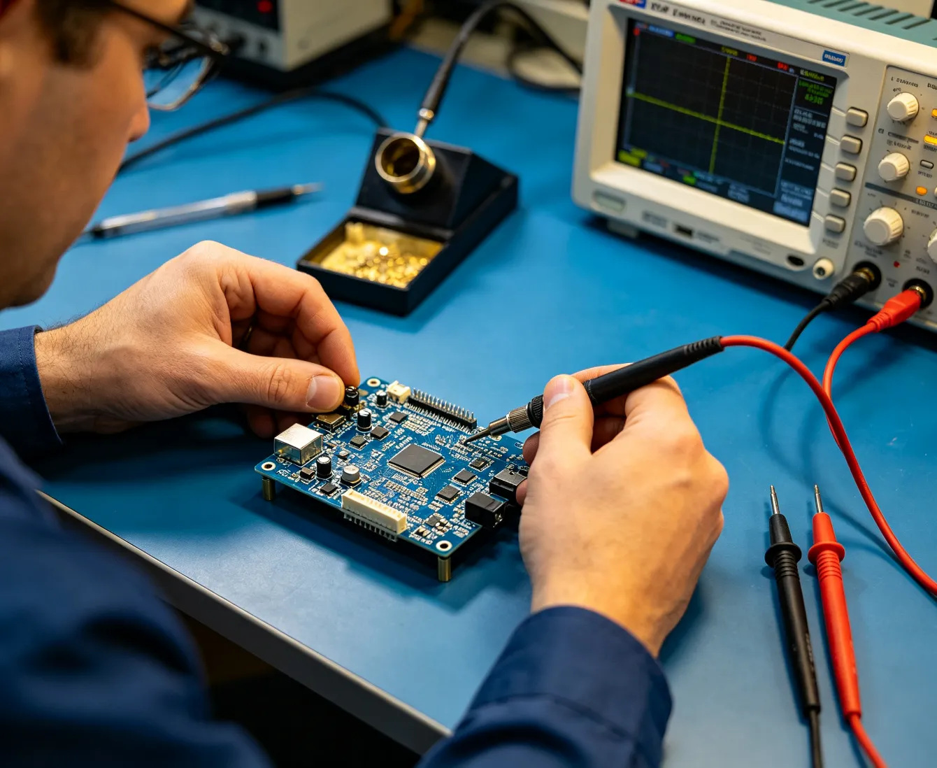
A PCB design that passes an engineering review is not automatically ready for manufacturing. The real test comes when the design is fabricated, assembled, powered, tested, and exposed to the conditions it will face in the finished product. Engineering validation supports this transition by identifying technical and production risks before they become expensive quality problems.
From our experience, the most costly electronics production problems are often not caused by one obviously bad design decision. They develop when several small issues interact: a component footprint has insufficient clearance, a high-speed signal has inadequate routing margin, a thermal assumption proves unrealistic, or an assembly process cannot consistently reproduce the intended result.
For engineering teams, OEMs, and procurement managers, validation should be treated as a production-readiness activity—not simply a final inspection step. The earlier critical assumptions are tested, the more control a business has over cost, delivery, reliability, and product performance.

Quick Answer: How Engineering Validation Supports Production
Engineering validation supports successful electronics production by checking whether a product design can meet its electrical, mechanical, thermal, reliability, and manufacturing requirements before large-scale production begins. It combines design reviews, simulation, prototype testing, PCB verification, assembly trials, and documented test results to reduce the risk of defects and costly redesigns.
Our recommendation: Validate the highest-risk functions and manufacturing constraints before approving production tooling, long-lead components, or volume orders. A controlled prototype and pre-production build are usually far less expensive than correcting a design problem after hundreds or thousands of units have been assembled.
Direct Answer: What Does Engineering Validation Actually Achieve?
Engineering validation establishes evidence that an electronics design works as intended and can be manufactured consistently under defined operating conditions. It connects engineering decisions with the practical requirements of PCB fabrication, component sourcing, SMT assembly, testing, and final product integration.
For example, a company developing an industrial controller may confirm that its PCB operates correctly on a laboratory bench. That is a useful first result, but it does not prove that the board will remain stable under temperature variation, electrical noise, vibration, repeated power cycles, or production assembly variation.
Engineering validation closes that gap. It asks whether the design meets its requirements, whether the selected manufacturing process can reproduce it, and whether the resulting product has enough margin to operate reliably.
Quick Summary: Engineering Validation at a Glance
| Area | What Is Checked | Production Benefit | When to Prioritize It |
|---|---|---|---|
| Electrical validation | Voltage, current, timing, signal integrity, power integrity | Reduces functional failures and electrical instability | Before design release and prototype approval |
| PCB design validation | Stack-up, impedance, spacing, materials, drill and routing constraints | Improves fabrication feasibility and board performance | Before PCB fabrication |
| Thermal validation | Component temperatures, heat dissipation, thermal margins | Reduces overheating and premature component degradation | Before enclosure and cooling design are finalized |
| Mechanical validation | Dimensions, connectors, mounting, fit, vibration exposure | Prevents integration and assembly problems | During prototype and system integration |
| Assembly validation | Component placement, soldering, reflow, inspection and process capability | Reduces repeatable SMT and assembly defects | Before production ramp-up |
| Reliability validation | Environmental stress, operating cycles, endurance and failure modes | Improves confidence in long-term product performance | Before product qualification and release |
1. What Is Engineering Validation in Electronics Production?
Engineering validation is a structured process for confirming that an electronic product, its PCB design, and its associated manufacturing approach satisfy defined technical and application requirements. It uses measurable evidence rather than relying solely on design assumptions or visual approval.
Depending on product complexity, validation may involve:
Design reviews: Checking schematics, PCB layouts, component selections, tolerances, and design documentation.
Engineering simulation: Evaluating electrical behavior, thermal performance, mechanical stress, or signal integrity before physical builds.
Prototype testing: Confirming that early boards operate according to their functional requirements.
Manufacturing feasibility reviews: Assessing whether the PCB and assembly design can be produced with the selected processes.
Reliability testing: Evaluating performance under relevant environmental, electrical, and operating stresses.
Production process checks: Confirming that inspection and test methods can detect important defects consistently.
The scope should reflect the actual risk. A simple low-speed control board does not require the same validation program as a high-speed communication board, semiconductor test interface, or safety-critical industrial system.
What Engineering Validation Is Not
Validation is not simply checking that a PCB powers on. It is also not a substitute for quality control, incoming inspection, or production testing. Those activities may reveal defects, but validation should establish whether the design and process are capable of meeting requirements in the first place.
2. How Engineering Validation Works: A Practical Process
A reliable validation process begins before the first prototype order. Engineering, manufacturing, procurement, and quality teams should agree on what must be proven and what evidence is sufficient for release.
Define requirements and acceptance criteria.
Document operating voltage, current limits, interface speeds, environmental conditions, mechanical dimensions, expected service life, and applicable regulatory or industry requirements. Avoid vague requirements such as "high reliability" without measurable acceptance criteria.
Review the schematic, BOM, and PCB layout.
Check component ratings, footprints, pin assignments, tolerances, clearances, routing, stack-up, and design-for-manufacturing considerations. Verify that the bill of materials matches the intended design revision.
Assess manufacturing feasibility.
Review whether trace widths, spacing, copper weights, via structures, board thickness, materials, and surface finishes are compatible with the intended PCB fabrication process. For assembly, assess package pitch, component orientation, placement access, and soldering requirements.
Build and inspect engineering prototypes.
Fabricate a controlled prototype batch and inspect it before assembly. Confirm dimensions, layer construction, critical features, and other agreed acceptance requirements. Record deviations rather than relying on informal approval.
Test electrical and functional performance.
Measure the parameters that matter to the application. This may include power-up behavior, signal timing, impedance, interface performance, noise, current consumption, and operation across specified load conditions.
Validate assembly and integration.
Run a representative assembly build, verify soldering and component placement, and confirm that the PCB fits the enclosure and connects correctly with other system components.
Complete risk-based reliability testing.
Use appropriate temperature, humidity, vibration, thermal cycling, endurance, or other stress tests where the application justifies them. Testing should reflect actual product risks, not an arbitrary checklist.
Review results and authorize production.
Close critical issues, approve the correct documentation revision, define production inspection points, and obtain formal sign-off from responsible stakeholders before volume manufacturing.
From our experience, the most useful validation records are those that connect each requirement to a test method, acceptance limit, result, and responsible reviewer. This makes engineering decisions traceable and helps prevent unresolved prototype issues from being forgotten during a production handover.
3. Key Benefits of Engineering Validation
Reduce Expensive Redesigns
A PCB revision after production release can involve more than a new board layout. It may require new fabrication, component procurement, assembly setup, testing, documentation, and customer approval. Catching a footprint, impedance, or thermal issue during engineering validation can avoid a much larger correction later.
Improve Manufacturing Yield
Some production defects originate in designs that are technically functional but difficult to manufacture consistently. Tight component spacing, unsuitable pad geometry, insufficient soldering clearance, or unrealistic tolerances can increase defect rates. Design-for-manufacturing reviews help identify these risks before the production line is committed.
Protect Product Reliability
Electrical margins, temperature limits, component derating, and mechanical stresses all influence product life. Validation helps confirm that a board is not merely functional under ideal laboratory conditions but is also appropriate for its intended operating environment.
Make Production Planning More Predictable
When engineering requirements and manufacturing constraints are reviewed early, procurement and production teams can make better decisions about materials, lead times, test fixtures, and process requirements. This is particularly important for projects with expensive components or tight delivery commitments.
Improve Communication Between Engineering and Manufacturing
A documented validation process gives engineers, PCB fabricators, assembly providers, and quality teams a shared basis for decisions. It reduces the risk of assumptions being transferred informally between departments or suppliers.
4. Limitations: What Engineering Validation Cannot Guarantee
Engineering validation is valuable, but it is not a promise that every future unit will be defect-free. A successful test demonstrates performance under the conditions and sample sizes evaluated. It cannot automatically cover every possible component variation, operating environment, handling issue, or process change.
| Limitation | Why It Matters | Practical Response |
|---|---|---|
| Limited sample size | A small prototype batch may not reveal low-frequency defects. | Use risk-based sampling and production monitoring. |
| Incomplete test conditions | Laboratory conditions may not represent actual field use. | Derive test conditions from the product's operating environment. |
| Component and material variation | Supplier or lot variation can affect performance. | Define approved parts, tolerances, and change-control requirements. |
| Process changes after approval | A validated design may behave differently after a manufacturing change. | Review significant process changes and revalidate where necessary. |
| Cost and schedule impact | Extensive testing can consume time and budget. | Prioritize high-risk functions and use staged validation. |
We do not recommend testing everything equally. A better approach is to identify failure modes with the greatest impact on safety, functionality, customer experience, and production cost, then allocate validation effort accordingly.
5. Who Should Use Engineering Validation?
For OEMs and Electronics Product Developers
OEMs should use engineering validation whenever a PCB is part of a product that must meet defined electrical, mechanical, or environmental requirements. It is especially important when the product has multiple interfaces, high component density, demanding operating conditions, or a costly field failure.
For PCB Design and Engineering Teams
Engineering teams should validate critical design assumptions before releasing fabrication files. This includes stack-up, impedance requirements, component footprints, routing constraints, thermal behavior, and design revisions. For high-speed applications, a review of high-speed PCB design and manufacturing considerations is particularly important.
For PCB Procurement and Manufacturing Managers
Procurement teams should not treat the lowest quoted PCB price as proof of production suitability. They need to confirm that the supplier understands the drawings, material requirements, tolerances, inspection expectations, and delivery constraints. Manufacturing managers should also confirm that the assembly process is appropriate for the selected components and board construction.
For Beginners
For beginners developing a simple prototype, a full qualification program may be unnecessary. However, a basic design review, prototype inspection, functional test, and manufacturing feasibility check are still worthwhile. The goal is to avoid preventable errors without creating an oversized validation process.
Who May Not Need Extensive Validation?
A low-risk, one-off experimental circuit may not justify formal environmental or endurance testing. If failure has little commercial impact and the board is not intended for repeated production, a focused functional check may be sufficient. Once the project moves toward customer delivery or volume manufacturing, the validation scope should increase.
6. Engineering Validation vs. Testing vs. Inspection
These terms are often used as if they mean the same thing. They do not. A mature electronics production process uses each activity for a different purpose.
| Activity | Main Question | Typical Methods | When It Happens |
|---|---|---|---|
| Engineering validation | Will the design and product meet real application needs? | Requirements review, prototype evaluation, system testing, environmental testing | During development and before release |
| Design verification | Does the design meet its specified requirements? | Calculation, simulation, analysis, test against specifications | Throughout design development |
| Manufacturing validation | Can the process consistently produce conforming units? | Trial builds, process checks, inspection, process capability studies | Before and during production ramp-up |
| Production testing | Does this individual unit function according to defined criteria? | Functional testing, in-circuit testing, boundary scan where applicable | During production |
| Quality inspection | Does the item meet specified acceptance criteria? | Visual inspection, dimensional checks, AOI, X-ray where appropriate | Incoming, in-process, and final inspection |
Our recommendation is to define these activities separately in the project plan. A board passing automated optical inspection does not prove that its high-speed interface meets signal-integrity requirements. Similarly, a functional test cannot replace a review of whether the PCB design is manufacturable at the intended volume.
7. PCB Engineering Validation: What Deserves the Most Attention?
The PCB is the physical foundation connecting electronic components and system interfaces. Its construction and layout directly influence electrical performance, assembly feasibility, and reliability. The validation priorities should reflect the board's complexity and intended use.
PCB Stack-Up and Material Selection
Layer count, dielectric thickness, copper weight, laminate properties, and overall board thickness should be reviewed against the electrical and mechanical requirements. For high-speed or RF designs, material selection and stack-up control can directly affect impedance and signal behavior.
For applications requiring controlled electrical performance, discuss the material and stack-up requirements with the fabricator before releasing the design. Do not assume that a generic FR-4 construction will automatically satisfy every frequency, loss, or thermal requirement.
Signal Integrity and Power Integrity
High-speed interfaces may be affected by impedance discontinuities, crosstalk, return-path interruptions, excessive via stubs, and poor routing topology. Power distribution networks can suffer from voltage drop, transient noise, or inadequate decoupling.
For commercial users developing high-speed electronics, simulation and design review should be completed before prototype fabrication whenever the risk justifies it. A board that works at a reduced data rate may not have sufficient margin at the required operating speed.
Thermal Management
Power components, processors, drivers, and dense component areas can create local hot spots. Validation should consider operating load, ambient temperature, copper distribution, thermal vias, heatsinks, and enclosure airflow. Thermal performance should be measured under representative conditions rather than inferred from component datasheets alone.
Manufacturing Tolerances and Design Rules
Trace width, spacing, annular ring, hole size, solder mask clearance, and board outline tolerances need to be compatible with the manufacturing capability agreed for the project. The goal is not to use the smallest possible dimensions. It is to use dimensions that meet the electrical requirements while remaining practical to fabricate.
Specialized PCB Technologies
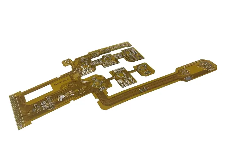
Different applications require different validation priorities. Flexible circuits need attention to bend radius, copper type, and mechanical stress. Semiconductor packaging and test applications may require tighter dimensional and electrical controls. For example, teams working with flexible PCB technology should evaluate repeated bending and assembly handling, while advanced packaging projects may need to review FC-CSP PCB or interposer PCB requirements at the early engineering stage.
For semiconductor test systems, validation may also involve specialized interface boards such as probe card PCBs, load board PCBs, and semiconductor test PCBs. These applications should be reviewed against their specific electrical, mechanical, and test-system requirements rather than treated like ordinary low-complexity boards.
8. How SMT PCB Assembly Validation Supports Production Readiness
A validated PCB design can still encounter problems during assembly. Component packages, solder paste deposition, placement accuracy, reflow profiles, board warpage, and inspection coverage all influence the final result.
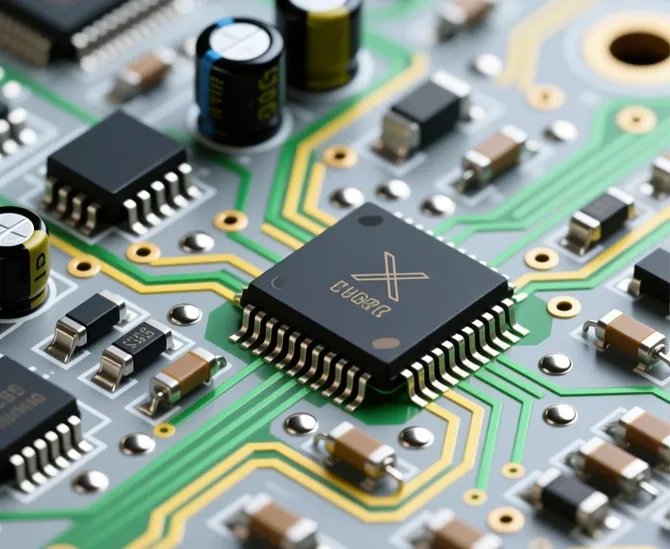
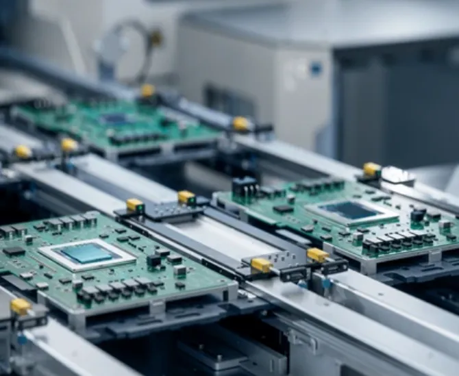
Surface Mount Technology (SMT) assembly places electronic components directly onto PCB pads. Automated SMT lines can provide speed and repeatability, but automation does not compensate for poor pad design, unsuitable component selection, or incomplete process requirements.
365PCB SMT PCB Assembly Services
365PCB provides professional SMT PCB assembly services using automated SMT lines for prototype and volume production. The service supports projects involving 0402 chip components, fine-pitch ICs, and BGA packages, with lead-free RoHS and leaded soldering options.
For projects that need a manufacturing partner, 365PCB's SMT capability can support the transition from PCB design and prototype builds to assembled boards. The company describes its service as having no minimum order quantity, which can be useful when evaluating early-stage builds before committing to larger production volumes.
What Should Be Validated Before an SMT Production Run?
Component and footprint compatibility: Confirm package dimensions, polarity, pin orientation, and land patterns against the approved BOM and PCB files.
Assembly documentation: Check the centroid file, assembly drawing, BOM, revision information, and special process instructions.
Solderability and pad design: Review pad geometry, solder mask openings, paste requirements, and fine-pitch spacing.
Reflow compatibility: Confirm that the selected components and PCB materials are compatible with the agreed soldering profile.
Inspection strategy: Determine whether AOI, X-ray, visual inspection, electrical testing, or other methods are appropriate for the assembly.
Traceability: Establish how component lots, board revisions, and production batches will be recorded when required.
For BGA packages, visual inspection alone cannot reveal every solder-joint issue. X-ray inspection may be appropriate depending on package design, risk, and customer requirements. The inspection plan should be agreed before production rather than decided after a defect is found.
We recommend treating the first assembled batch as a process-learning opportunity. Review defects, rework, placement issues, and test failures before approving a larger production run.
9. Comparison Table: Validation Approaches for Different Electronics Projects
There is no single validation plan that suits every PCB. The right approach depends on technical complexity, production volume, application risk, and the cost of failure.
| Project Type | Recommended Validation Scope | Priority Risks | Our Recommendation |
|---|---|---|---|
| Simple low-speed PCB | Design review, prototype function test, basic manufacturing review | Incorrect footprints, polarity, assembly errors | Keep validation focused, but never skip the prototype check. |
| Industrial control PCB | Electrical, thermal, mechanical, environmental and functional evaluation | Temperature, electrical noise, operating cycles, field reliability | Validate under representative operating loads and environmental conditions. |
| High-speed PCB | Stack-up review, impedance control, SI/PI analysis, prototype measurement | Signal integrity, crosstalk, loss, power noise | Resolve critical routing and material questions before fabrication. |
| Flexible PCB | Electrical, dimensional, bending and assembly validation | Copper fatigue, bend radius, connector stress | Test the actual mechanical movement and assembly conditions. |
| Semiconductor test PCB | Electrical performance, dimensional accuracy, interface and application-specific testing | Contact alignment, signal behavior, repeatability | Define interface requirements and acceptance criteria with the test-system team. |
| High-volume SMT product | Prototype assembly, process trial, inspection and production test validation | Solder defects, placement variation, yield and traceability | Approve the process using a representative pre-production build. |
10. Common Engineering Validation Mistakes
Mistake 1: Treating a Successful Power-On as Full Validation
A board powering on proves only that it has passed one basic milestone. It does not confirm performance under full load, temperature variation, interface stress, or long-term operation. Define tests around actual requirements, not just whether the prototype appears to work.
Mistake 2: Reviewing the PCB Without Consulting the Manufacturer
Engineering teams sometimes release a design without confirming fabrication constraints. This can result in avoidable questions, delays, or design changes. Discuss unusual stack-ups, tight tolerances, controlled impedance, and special materials with the manufacturer before production files are finalized.
Mistake 3: Using an Incomplete BOM
Missing manufacturer part numbers, package details, approved alternatives, or lifecycle information can create sourcing and assembly uncertainty. A BOM should be controlled and consistent with the schematic, layout, and assembly documentation.
Mistake 4: Skipping the Assembly Prototype
An unassembled bare PCB cannot reveal every SMT process issue. Fine-pitch components, BGAs, mixed package sizes, and dense layouts should be evaluated through a representative assembly build where appropriate.
Mistake 5: Changing Materials or Processes Without Review
Replacing a laminate, surface finish, component, or soldering process may affect performance. Any change that could influence a critical requirement should be assessed through a documented engineering change process.
Mistake 6: Failing to Define Acceptance Criteria
Statements such as "the signal should be stable" or "the board must be reliable" are not sufficient. Define measurable limits, test conditions, and pass/fail rules before testing begins.
Mistake 7: Ignoring Production Feedback
Validation should not end when the first production order ships. Yield data, inspection results, customer feedback, and field returns can reveal risks that were not visible during prototype development. Use this information to improve future revisions and process controls.
11. How to Choose a PCB Manufacturer That Supports Engineering Validation
A capable PCB manufacturer should do more than accept Gerber files and issue a price. The supplier should be able to review technical requirements, identify manufacturing concerns, clarify unclear documentation, and explain how critical features will be controlled.
Evaluate Technical Capability, Not Just Equipment Lists
Ask whether the manufacturer has relevant experience with your board type, material, layer count, tolerances, and surface finish. For advanced applications, ask how the supplier manages stack-up review, impedance requirements, drilling, plating, and dimensional inspection.
Check Engineering Communication
Before placing an order, submit a representative design package and assess the quality of the technical feedback. A useful engineering response should identify specific questions or risks, not simply confirm that the files have been received.
Review Quality Systems and Inspection Capability
Ask how the supplier controls production revisions, material traceability, inspection records, and nonconforming products. Depending on the application, review the relevance of IPC workmanship requirements, ISO 9001 quality management, and other customer or industry-specific standards.
Confirm Prototype-to-Production Support
A supplier that can support both prototype and production stages may simplify communication and reduce handover friction. However, confirm that the same approved specifications, materials, and process requirements will be maintained when volume increases.
Use a Structured Supplier Comparison
| Evaluation Factor | What to Ask | Warning Sign |
|---|---|---|
| Engineering review | Can the supplier review the design and raise manufacturability concerns? | Only accepts files without technical clarification. |
| Relevant technology | Has the supplier manufactured similar PCB structures and materials? | Promises every capability without explaining process limits. |
| Quality control | What inspection and test records are available? | Cannot explain acceptance criteria or defect handling. |
| Revision management | How are design changes and production revisions controlled? | Unclear version tracking or undocumented substitutions. |
| Delivery planning | What are the material, fabrication, assembly, and test lead times? | Quotes a delivery date without reviewing project complexity. |
| Commercial transparency | Are tooling, testing, engineering, and expedite costs clearly identified? | Low headline price with unclear additional charges. |
For teams preparing a new project, 365PCB provides an online PCB instant quote service to support early cost evaluation. For a useful quotation, provide complete fabrication data, board specifications, quantities, required delivery dates, and any special validation or inspection requirements.
12. Cost-Benefit Analysis: Is Engineering Validation Worth the Investment?
For most commercial electronics projects, the answer is yes—provided the validation scope is proportionate to the risk. The cost of validation is visible in the project budget. The cost of inadequate validation is often hidden until a production delay, field failure, rework campaign, or customer complaint occurs.
Where Validation Creates Financial Value
Fewer engineering change orders: Early discovery can reduce repeated PCB fabrication and assembly cycles.
Lower rework exposure: Better pad design, component selection, and process planning can reduce avoidable assembly issues.
Less production disruption: A pre-production build can reveal process constraints before the line is committed to volume.
Reduced field failure risk: Application-relevant testing can identify weaknesses before products reach customers.
Better supplier coordination: Clear requirements reduce ambiguity in quotations, manufacturing, and quality acceptance.
Example: Prototype Cost vs. Production Rework
Consider a hypothetical project that plans to manufacture 2,000 assembled control boards. A prototype validation stage identifies an unsuitable connector footprint and a thermal issue near a power component. Correcting both before production may require another design revision and a limited prototype build.
If the same issues are discovered after volume assembly, the project may face board replacement, component removal, reassembly, retesting, delayed delivery, and possible customer-side costs. The exact financial impact depends on the product and process, but the commercial principle is straightforward: early engineering evidence gives the team more options and usually lowers the cost of correction.
Where to Spend the Validation Budget First
We recommend prioritizing the following:
Safety-related and high-consequence functions.
High-speed, high-current, or thermally demanding circuits.
Hard-to-source or expensive components.
Complex packages such as fine-pitch ICs and BGAs.
Special PCB materials, structures, or tight manufacturing tolerances.
Processes that will be difficult or expensive to change after production starts.
For a straightforward prototype, a focused review and functional test may be enough. For heavy-duty applications, high-volume manufacturing, or products with expensive field failures, a more complete validation program is usually justified.
13. Pros and Cons of Engineering Validation
| Pros | Cons |
|---|---|
| Identifies design and manufacturing risks before volume production. | Requires additional engineering time and project planning. |
| Improves confidence in electrical, thermal, and mechanical performance. | Some tests require specialized equipment or external laboratories. |
| Can reduce rework, redesign, and production disruption. | May add prototype or pre-production build costs. |
| Creates traceable evidence for design and production decisions. | Results are limited to the conditions and samples evaluated. |
| Improves communication between OEMs, PCB manufacturers, and assembly teams. | Requires disciplined documentation and change control. |
The disadvantages are manageable when validation is planned around risk. The wrong approach is to test everything without a clear objective. The right approach is to identify what could cause a serious failure, define how to detect it, and collect enough evidence to make a confident production decision.
14. Expert Recommendation: Build Validation Into the Production Plan
Engineering validation should be a defined project milestone, not an informal activity squeezed between prototype delivery and mass production. The most effective approach is staged: verify the design, validate the application, confirm manufacturing feasibility, and then approve production using documented results.
For Beginners
Start with a complete schematic and BOM review, confirm PCB manufacturability, build a small prototype batch, and test the board's core functions. Do not order a large quantity simply because the first board powers on.
For Commercial Users
Require clear acceptance criteria, controlled design revisions, supplier engineering feedback, and a representative pre-production build. Make sure procurement, engineering, and quality teams agree on what constitutes production readiness.
For High-Speed and Advanced PCB Applications
Resolve stack-up, impedance, signal integrity, material, and manufacturing tolerance questions before fabrication. Specialized designs such as IC substrate PCBs and SiP PCBs deserve early technical coordination because their packaging and electrical requirements can leave little room for late-stage changes.
For Heavy-Duty and Long-Life Products
Give thermal, environmental, mechanical, and component lifecycle risks appropriate attention. A design that works under a short laboratory test may still be unsuitable for continuous operation in a demanding environment.
Frequently Asked Questions About Engineering Validation
1. What is engineering validation in electronics manufacturing?
Engineering validation is the process of confirming that an electronic product and its design meet defined application requirements. It may include design reviews, simulation, prototype testing, PCB inspection, assembly trials, functional testing, and reliability evaluation.
2. Why is engineering validation important before mass production?
It helps identify electrical, thermal, mechanical, and manufacturing problems before they affect large production quantities. This can reduce redesign costs, assembly defects, delivery delays, and field failures.
3. What is the difference between design verification and design validation?
Design verification checks whether a design meets its specified requirements. Design validation checks whether the resulting product meets the needs of its intended application. Both are important, but they answer different questions.
4. Does every PCB project need engineering validation?
Every PCB project benefits from an appropriate level of review and testing, but the scope should match the risk. A simple prototype may need basic functional and manufacturing checks, while complex or high-volume products require more extensive validation.
5. What should be checked during PCB engineering validation?
Important checks include PCB stack-up, material selection, trace width and spacing, impedance requirements, component footprints, thermal behavior, mechanical dimensions, manufacturing tolerances, and electrical performance.
6. How does SMT assembly validation reduce production defects?
It evaluates whether component placement, solder paste, reflow conditions, package selection, inspection, and testing are suitable for the design. A representative assembly build can expose issues before volume manufacturing begins.
7. When should engineering validation take place?
Validation should begin during design development and continue through prototype testing, manufacturing feasibility review, assembly evaluation, and production release. High-risk requirements should be checked as early as practical.
8. Can a PCB manufacturer help with engineering validation?
Yes. A capable manufacturer can review fabrication data, identify manufacturing constraints, clarify material and stack-up requirements, and support prototype or pre-production builds. Product-level functional and application validation may still require the OEM's engineering team.
9. Which standards are relevant to electronics engineering validation?
The applicable standards depend on the product and industry. Common references include IPC standards for PCB design and assembly workmanship, ISO 9001 for quality management systems, and product-specific safety or environmental standards. The project team should identify the applicable requirements rather than assume one standard covers every validation need.
10. How can I reduce the cost of engineering validation?
Prioritize tests based on risk, use simulation where it can answer meaningful questions, review manufacturability before ordering prototypes, and define acceptance criteria early. Avoid unnecessary testing, but do not remove checks that protect critical product functions or expensive production commitments.
References and Industry Standards
The following authoritative resources provide useful background for quality management, PCB design, and electronics assembly requirements. Always confirm the current edition and contractual applicability before using a standard as a project acceptance requirement.
ISO 9001:2015 – Quality Management Systems. International Organization for Standardization. A framework for quality management, process control, and continual improvement.
IPC – Association Connecting Electronics Industries. Industry standards and technical resources covering PCB design, fabrication, assembly, and electronic product acceptance.
National Institute of Standards and Technology (NIST). Technical resources on measurement science, engineering standards, testing, and manufacturing quality.
Plan Your Next PCB Project With Manufacturing in Mind
Successful electronics production starts with a design that has been reviewed against real manufacturing and application requirements. Whether you are developing a prototype, refining a high-speed board, or preparing an SMT production run, early technical coordination can prevent avoidable problems later.
365PCB supports PCB fabrication and SMT assembly requirements for engineering and commercial projects. Share your PCB files, specifications, quantity, and technical requirements to begin a manufacturing review.
Request a PCB Instant Quote or explore 365PCB SMT PCB Assembly Services.