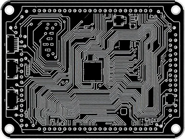
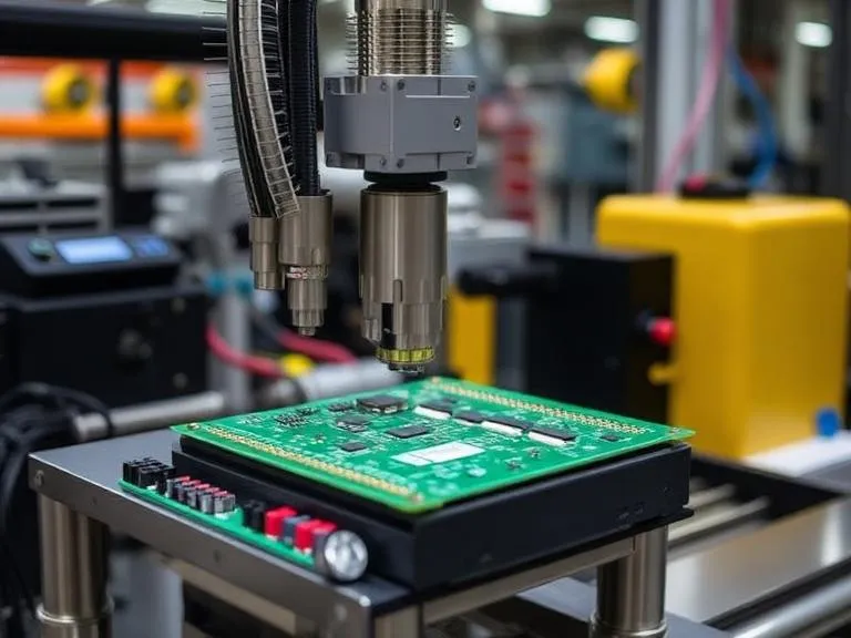
If you dismantle any modern electronic device—from a complex aerospace telemetry system to a simple household smart plug—you will inevitably find a rigid green, blue, or black board acting as the central nervous system of the hardware. The role of the PCB in electronics is absolute. It has entirely replaced the archaic, failure-prone point-to-point hand wiring of the mid-20th century. However, despite its ubiquity, many hardware entrepreneurs and junior engineers deeply misunderstand how these boards are engineered, leading to catastrophic signal failures and blown manufacturing budgets.
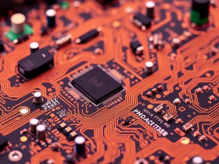
From our experience engineering and manufacturing millions of boards, viewing a printed circuit board as merely a "dumb" piece of fiberglass is the fastest way to ruin a product launch. A modern circuit board is a highly complex, carefully tuned electrical component in its own right. We wrote this guide to provide a brutal, clear-eyed commercial perspective on what these boards are, how the underlying physics govern their design, and how you should make strategic sourcing decisions for your hardware projects.
Quick Answer: What is a PCB?
A PCB (Printed Circuit Board) is the physical and electrical foundation of modern electronics. It is a laminated sandwich structure of non-conductive insulating material (typically fiberglass) and highly conductive copper layers. Instead of using bulky physical wires to connect components like microchips, resistors, and capacitors, a PCB uses precisely etched copper pathways (called traces) to route electrical signals and power. We recommend prioritizing professional PCB design over breadboards early in any commercial project to guarantee signal integrity, mechanical durability, and manufacturing scalability.
What It Is: The Anatomy of a PCB
To understand the function of a PCB in electronics, you must first deconstruct its physical layers. A standard rigid circuit board is not a single piece of material; it is a meticulously bonded composite cured under extreme heat and pressure.
At the core lies the substrate. In most professional situations, this is a flame-retardant fiberglass-epoxy composite. If you are building standard consumer electronics, utilizing a traditional FR4 PCB is the industry default. Laminated onto this substrate is a layer of copper foil. The thickness of this copper (usually measured in ounces per square foot) dictates how much electrical current the board can safely handle before overheating.
Covering the copper is the solder mask—the polymer layer that gives PCBs their iconic green color. The solder mask prevents accidental short circuits and insulates the copper traces from environmental oxidation. Finally, the silkscreen layer is printed on top, providing human-readable reference designators (like "R1" or "C4") to guide the assembly process.
Quick Summary Table: Core Layers of a PCB| Layer Name | Primary Material | Core Function |
|---|
| Substrate (Core) | Fiberglass Epoxy (FR4), Polyimide, or Metal | Provides physical rigidity and electrical insulation. |
| Conductive Layer | Copper Foil | Acts as the physical wire, routing power and data signals. |
| Solder Mask | Liquid Photoimageable Polymer (LPI) | Prevents solder bridges during assembly; protects copper. |
| Silkscreen | Epoxy Ink | Displays component labels, logos, and assembly instructions. |
How It Works: Electrical Routing and Vias
How does a PCB actually work? It functions by treating the copper layer as a blank canvas, from which unwanted copper is chemically etched away, leaving only the required electrical "highways" or traces. When a microchip needs to send a high-speed data signal to a memory module, the signal travels across these microscopic copper traces at near the speed of light.
However, complex electronics cannot fit all their wiring on a single flat plane without the traces crossing and short-circuiting. To solve this, manufacturers stack multiple layers of copper and substrate. A standard IoT device might require a 4-layer or 6-layer board. The magic of multi-layer boards relies on "vias"—microscopic holes drilled through the board and plated with copper. Vias act as elevator shafts, allowing an electrical signal to drop from layer 1 down to layer 4, bypass an obstacle, and pop back up to the surface.
As miniaturization accelerates, standard mechanical drilling becomes inadequate. Modern smartphones and wearables rely on an HDI PCB (High Density Interconnect), which utilizes laser-drilled microvias to pack an astonishing amount of computational power into a fraction of a square inch.
About China 365PCB
China 365PCB is a fully self-operated, full-industry-chain manufacturing group — from PCB fabrication, SMT assembly, online electronic component sourcing and integration, CNC machining, cable harness assembly, to complete OEM/ODM solutions.
With 15+ years of experience, 365PCB operates over 100,000㎡ of production area, all facilities are self-owned and self-managed, ensuring total quality control, full process traceability, and unmatched production flexibility.
With a one-stop turnkey service from design to delivery, we guarantee no delay, no excuses — truly realizing 365 days of fast manufacturing for global customers.
The Commercial Benefits
Why did the entire global electronics industry standardize on PCBs? The answer is consistency and scalability. When you move from a hand-wired prototype to a printed circuit board, you eliminate human wiring errors. Every single board off the manufacturing line possesses the exact same electrical characteristics.
Furthermore, PCBs optimize Signal Integrity (SI) and Electromagnetic Interference (EMI). In high-speed digital circuits, a stray wire acting as an antenna will crash the system. PCBs allow engineers to design solid copper ground planes that shield sensitive data lines from external noise, guaranteeing reliable operation in harsh environments.
Limitations and Engineering Constraints
The primary limitation of a PCB in electronics is its permanence. Once a board is etched and fabricated, you cannot easily alter the wiring. If you make a routing error in your design files, you must scrap the physical boards, correct the CAD file, and pay for a new manufacturing run. This introduces Non-Recurring Engineering (NRE) costs and tooling delays.
Additionally, rigid PCBs struggle with mechanical flexibility. If you are designing a wearable medical device or a folding smartphone, a rigid board will snap. In these scenarios, the limitation is overcome by upgrading the base material, but doing so drastically alters the cost matrix.
Pros and Cons Table: PCB Implementation| Advantages (Pros) | Disadvantages (Cons) |
|---|
| Massively scalable for automated robotic assembly (SMT). | High upfront NRE (tooling and setup) costs for low volumes. |
| Exceptional control over high-speed signal integrity. | Inflexible design; impossible to re-route once manufactured. |
| Compact size; allows for extreme miniaturization. | Thermal management requires careful engineering in high-power setups. |
| Highly reliable in vibration and high-impact environments. | Requires specialized CAD software knowledge to design correctly. |
Who Should Use It
For commercial users: Anyone intending to manufacture a physical electronic product for public sale must use a PCB. Regulatory bodies will not certify products that rely on loose wire-wrapping. Whether you are building 100 specialized medical sensors or 100,000 consumer Bluetooth speakers, PCBs are mandatory.
For beginners and hardware startups: As soon as your concept is proven, you must transition to a professional PCB Prototype Service. Do not attempt to pitch investors with a messy breadboard covered in jumper wires. A custom prototype board demonstrates engineering competence and manufacturing readiness.
Who Does Not Need It
You do not need to order a custom PCB if you are in the very first hour of testing a basic circuit theory. If you are a hobbyist hooking up an LED to a battery and a resistor just to see if it lights up, a solderless breadboard is the correct tool. Solderless breadboards allow for instant, infinite modifications without any financial cost. Only once the schematic is mathematically verified should you commit to a fabricated board.
Common Mistakes in PCB Design
In our testing and review of thousands of client Gerber files, the most expensive mistakes rarely involve complex routing; they involve a fundamental misunderstanding of material science. Engineers frequently ignore thermal stress.
If you are designing a high-power LED array or an industrial motor controller, a standard FR4 board will act as an insulator, trapping heat until the components melt off the pads. For heavy-duty applications managing high thermal loads, you must specify an Aluminum PCB to actively conduct heat away from the chips. Furthermore, for devices operating in extreme environments (like automotive under-the-hood sensors), failing to specify a High TG PCB will result in the board physically warping and delaminating as temperatures cross 150°C.
Comparison Table: Prototyping vs. Production Hardware| Platform | Best Use Case | Reliability | Cost per Unit (at scale) |
|---|
| Solderless Breadboard | Initial circuit theory testing. | Very Low (wires fall out) | N/A (Not for production) |
| 2 Layer PCB | Simple microcontrollers, analog audio, IoT sensors. | High | Extremely Low |
| Multi-Layer HDI PCB | Smartphones, dense computers, advanced RF. | Very High | Moderate to High |
Buying Considerations and Upgrades
When you are ready to make a buying decision, you must evaluate the mechanical constraints of your product enclosure. Does your circuit need to fit into a curved housing, like a smartwatch or an aerospace camera gimbal?
If space is tight and dynamic bending is required, you must abandon rigid boards and upgrade to an FPC PCB (Flexible Printed Circuit). If your design requires the rigid strength to hold heavy microprocessors but the flexibility to fold around corners to connect to a display, a Rigid Flex PCB is the ultimate engineering solution. While rigid-flex boards have a higher upfront fabrication cost, they eliminate the need for heavy, expensive manual wiring harnesses and mechanical connectors, often resulting in a lower overall assembly cost.
Buying Guide Table: Selecting Your PCB Material| Application Requirement | Recommended PCB Type | Why Make This Upgrade? |
|---|
| Standard consumer electronics | Standard FR4 | Most cost-effective; proven industry standard. |
| High heat generation (LEDs, Power) | Aluminum / Metal Core | Superior thermal conductivity prevents component failure. |
| Tight spaces requiring folding | FPC PCB / Rigid-Flex | Eliminates bulky wire harnesses and saves weight. |
| Harsh environments / high temp reflow | High TG (170Tg or 180Tg) | Prevents physical board expansion and trace cracking. |
Expert Recommendation
From our experience managing full-lifecycle electronics manufacturing, our firm recommendation is to over-engineer your initial prototype materials and aggressively cost-down during mass production. Do not build your initial proof-of-concept on cheap, low-grade substrates. If you are unsure about the thermal dynamics of your new hardware, upgrade to a High TG material immediately to eliminate the substrate as a point of failure during your testing phase. Once the electrical design is validated, rely on a vertically integrated manufacturing partner to help you strip out unnecessary costs, optimize your layer stack-up, and scale gracefully into global mass production.
Frequently Asked Questions
What is the difference between a PCB and a PCBA?
A PCB (Printed Circuit Board) refers to the blank, unpopulated board containing only the fiberglass and copper traces. A PCBA (Printed Circuit Board Assembly) is the finished product after all the electronic components (microchips, resistors, capacitors) have been soldered onto the PCB.
Why are most PCBs green?
The green color comes from the liquid photoimageable (LPI) solder mask applied over the copper layers. Historically, green was the most chemically stable pigment and provided the best visual contrast for human inspectors to spot faults. Today, PCBs can be manufactured in almost any color, including matte black, white, red, or blue.
Can I fix a broken trace on a PCB?
In most professional situations, a damaged PCB trace in a mass-produced consumer item is not repaired because the labor cost exceeds the cost of a new board. However, for expensive industrial or prototype boards, a technician can meticulously scrape away the solder mask and bridge the broken trace with a fine gauge wire, known as a "bodge wire."
David Li
David Li is the Technical Communications Director at China 365PCB, with over 15 years of hands-on experience in the PCB and electronics manufacturing industry. Holding a Master’s degree in Electrical Engineering, he has worked extensively in both R&D and manufacturing roles at leading multinational electronics firms in Shenzhen before joining our team.
His expertise spans high-speed digital design, advanced packaging (HDI, Flex), and automotive-grade reliability standards. David is passionate about bridging the gap between design intent and production reality—a philosophy that aligns perfectly with 365PCB’s mission to deliver seamless, rapid, and fully-integrated manufacturing solutions.
Follow David’s insights on PCB technology trends and best practices here on the 365PCB Knowledge Hub.
 English