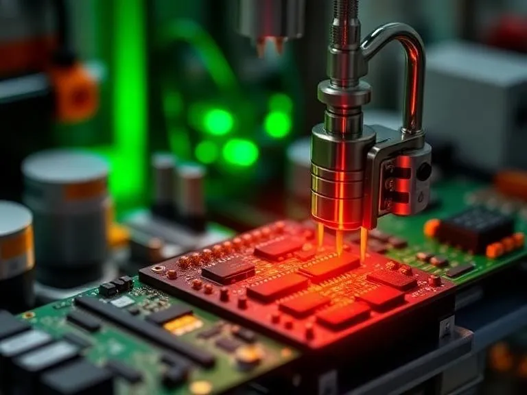
When hardware engineers and procurement managers evaluate a potential manufacturing partner, they often look at pricing, lead times, and marketing brochures. From our experience, this is the wrong approach. If you want to know the true capability, yield rate, and reliability of a factory, you must audit the equipment required for PCB manufacturing sitting on their production floor.
Building a high-density, multi-layer printed circuit board is an exercise in extreme chemical and mechanical precision. A single factory line requires tens of millions of dollars in capital investment. Whether you are seeking a reliable Custom PCB partner or trying to understand the physical constraints of your designs, knowing what machinery handles your Gerber files is critical.
Quick Answer: What Equipment is Required?
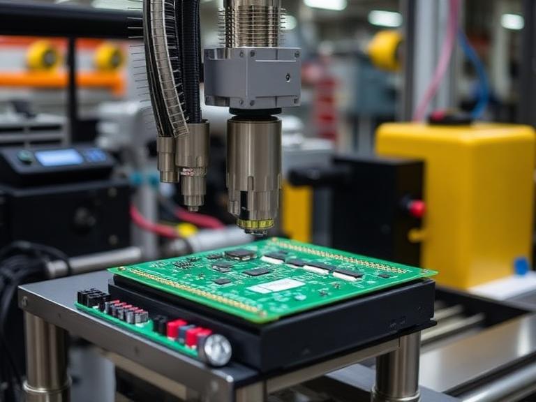
The core equipment required for PCB manufacturing includes Laser Direct Imaging (LDI) machines for photolithography, automated CNC mechanical and CO2 laser drills for via creation, Vertical Continuous Plating (VCP) lines for copper deposition, chemical etching machines, automated solder mask sprayers, and rigorous inspection systems such as Automated Optical Inspection (AOI) and Flying Probe Testers. The quality, age, and automation level of this equipment dictate whether a facility can produce complex High-Density Interconnect (HDI) boards or only basic single-layer prototypes.
1. Quick Summary Table: Core PCB Machinery
In most professional situations, a fully integrated facility must operate the following core machines to control quality from raw material to final test.
| Equipment Type | Primary Function | Quality Indicator (What to look for) |
|---|
| Laser Direct Imaging (LDI) | Exposes the circuit pattern onto photoresist. | Replaces traditional film; achieves fine trace/space (under 3 mil). |
| CNC Drilling Machines | Drills mechanical through-holes and tooling holes. | Spindle speeds exceeding 160,000 RPM for precise micro-vias. |
| Laser Drills (CO2 / UV) | Vaporizes epoxy/glass for blind and buried vias. | Mandatory for HDI boards and micro-vias under 0.15mm. |
| VCP Plating Lines | Deposits copper into drilled vias for conductivity. | Vertical Continuous Plating ensures even distribution. |
| AOI Machines | Optically inspects etched copper for shorts/opens. | High-resolution cameras tied to AI defect recognition. |
| Flying Probe Testers | Electrically tests the finished board without fixtures. | Speed and accuracy for low-volume, high-mix runs. |
2. What It Is and How It Works: The Production Line
To understand the equipment required for PCB manufacturing, we must trace the chronological path of a raw FR4 panel through the factory floor.
Imaging: Laser Direct Imaging (LDI)
Historically, circuit patterns were printed on Mylar film, which was then placed over the copper panel and exposed to UV light. Film stretches, shrinks, and scratches. Today, modern factories use LDI. This machine works by taking the CAD data and using a highly focused UV laser to directly "draw" the circuitry onto the photoresist. This completely eliminates alignment errors caused by film distortion.
Drilling: CNC Mechanical and Laser Machining
A PCB is useless if the layers cannot communicate. Automated CNC drilling machines stack multiple panels and use carbide drill bits to create through-holes. For advanced designs, CO2 and UV laser drills are utilized to ablate (burn away) the dielectric material to form micro-vias without damaging the copper pad below it.
Chemical Wet Processing: Plating and Etching
Once drilled, the board goes through an electroless copper line, followed by electrolytic plating (often a Vertical Continuous Plating or VCP line). These massive chemical baths use electrical current to deposit copper uniformly inside the walls of the drilled holes. Afterward, etching lines use alkaline or acidic solutions to strip away the unwanted copper, leaving only the intended circuitry.
Inspection and Testing: AOI and Bed of Nails
Before applying the solder mask, the boards run through PCB Actual Board Area (AOI) machines. These optical scanners compare the physical etched copper against the original Gerber files. After final surface finishes are applied, the boards undergo a rigorous PCB Electrical Testing Service using either Flying Probe machines (for prototypes) or custom Bed of Nails fixtures (for high volume).
3. Benefits of Tier-1 Manufacturing Equipment
Why do industry leaders invest tens of millions in upgrading their equipment required for PCB manufacturing? We recommend partnering with highly equipped factories because of three distinct benefits:
Uncompromising Reliability: Automated VCP plating lines ensure the copper thickness inside a via is perfectly uniform. Manual dip lines often result in thin via walls that crack under thermal stress during assembly.
Tight Tolerances: LDI equipment allows for trace and space widths down to 2/2 mils. This is non-negotiable for modern BGA (Ball Grid Array) component routing.
Process Traceability: Modern machinery logs exact chemical temperatures, drill hit counts, and exposure times. If a failure occurs in the field, a factory with modern equipment can trace the exact batch and machine parameter that caused it.
4. Limitations of Budget Factory Setups
The stark reality of the PCB industry is that many "manufacturers" you find online are actually brokers, or they operate aging, depreciated equipment to offer bottom-barrel prices. The limitations of legacy equipment are severe. Mechanical routing machines with worn spindles leave rough edges and fiberglass dust. Older etching lines suffer from "puddle effects," causing over-etching on the top of the board and under-etching on the bottom.
For heavy-duty applications, such as an Automotive PCB where failure can result in loss of life, trusting a facility that lacks automated chemical control systems and high-end AOI is a catastrophic commercial risk.
5. Pros vs Cons: Automated vs Manual Lines
When evaluating the equipment required for PCB manufacturing, buyers must understand the shift from manual intervention to full automation.
| Fully Automated Equipment Lines | Manual / Semi-Automated Lines |
|---|
| Pro: Zero human handling reduces contamination and oxidation. | Pro: Much lower capital expenditure, allowing for cheaper unit prices. |
| Pro: Exact chemical dosing maintains perfect plating thickness. | Pro: Highly flexible for strange, non-standard experimental materials. |
| Con: Requires massive facility space and extreme capital investment. | Con: Operator fatigue leads to severe inconsistency batch-to-batch. |
| Con: Costly to shut down and start up; favors continuous operation. | Con: Cannot achieve the precision required for HDI or fine-pitch BGAs. |
6. Who Should Care About This List (And Who Does Not Need It)
Who should actively audit equipment: Procurement managers, NPI (New Product Introduction) engineers, and hardware founders. If you are transitioning from prototype to a High-Volume Production PCB run, you absolutely must verify that your chosen partner actually owns the laser drills and VCP lines they claim to have. If they outsource the drilling or plating, you lose control of your supply chain.
Who does not need it: For beginners or hobbyists building simple 2-layer Arduino shields with 10-mil traces, the specific brand of the CNC drill at the factory is irrelevant. Almost any legacy equipment can produce a basic 2-layer board successfully.
7. Common Mistakes Buyers Make During Factory Audits
From our experience hosting hundreds of global clients at our 100,000㎡ production facility, we see buyers make the same mistakes when evaluating the equipment required for PCB manufacturing:
Ignoring the "Wet" Processes: Buyers love to look at the fast-moving CNC drills, but they ignore the chemical plating and etching lines. Wet processing is where 80% of PCB failures (like via cracking or delamination) originate. Look for automated dosing systems.
Falling for the "We Can Do It" Trap: A factory might say they can do a Hard Gold PCB surface finish. But do they have an in-house hard gold plating line, or are they putting your boards on a truck to a subcontractor across town? Outsourcing critical steps ruins lead times.
Failing to Check Testing Equipment Calibration: A Flying Probe tester is useless if its calibration is out of date. Always verify the age and maintenance schedule of inspection equipment.
8. Comparison: Legacy Equipment vs. Modern Equipment
| Manufacturing Step | Legacy Equipment Setup | Modern Tier-1 Setup |
|---|
| Image Transfer | Mylar Film & UV Contact Printers | Laser Direct Imaging (LDI) |
| Micro-via Drilling | Mechanical drill (limits to 0.2mm, high wear) | CO2 / UV Laser ablation (sub 0.1mm accuracy) |
| Copper Plating | Manual hoist and dip tanks | Vertical Continuous Plating (VCP) automation |
| Solder Mask | Manual screen printing | Automated spray coating and LED curing |
9. Buying Considerations: Evaluating a Factory
For commercial users, you are not buying the equipment yourself; you are buying access to it. Use this buying guide to interview your next PCB manufacturing partner.
| What to Ask the Manufacturer | Why It Matters to Your Product |
|---|
| "Is your entire facility self-owned and self-operated?" | Brokers add margins and lose control over quality. You want a direct factory with all equipment under one roof. |
| "Do you use LDI for all multi-layer boards?" | Ensures your complex traces won't suffer from film-shift shorts. |
| "How do you handle rapid prototyping?" | A good partner has dedicated Quick Turn PCB equipment lines so prototypes don't interrupt mass production. |
| "Do you have in-house testing?" | Verifies that they are not shipping boards blindly. AOI and Flying Probe must be in-house. |
10. Expert Recommendation from China 365PCB
Our Stance: Never trust a manufacturer who relies heavily on subcontracting. The PCB manufacturing process is entirely interdependent. If the drilling equipment is misaligned, the plating line will fail to coat the vias properly.
At China 365PCB, we have built a fully self-operated, full-industry-chain manufacturing group. With over 15 years of experience, we operate over 100,000㎡ of production area. Every piece of equipment required for PCB manufacturing—from LDI and VCP lines to our SMT assembly and CNC machining centers—is strictly self-owned and self-managed.
This massive capital investment in our own equipment ensures total quality control, full process traceability, and unmatched production flexibility. By offering a one-stop turnkey service from design to delivery, we guarantee no delay and no excuses. We truly realize 365 days of fast, reliable manufacturing for our global customers.
11. Frequently Asked Questions (FAQ)
What is the most expensive equipment required for PCB manufacturing?
Laser Direct Imaging (LDI) machines and automated Vertical Continuous Plating (VCP) lines are generally the most capital-intensive pieces of equipment, often costing millions of dollars each. They are critical for high-yield, precise manufacturing.
Can I start a PCB factory in my garage?
While hobbyists can etch simple 1-layer or 2-layer boards using basic acid baths and a drill press, a commercial-grade, multi-layer PCB factory requires heavy industrial equipment, strict chemical waste management systems, and climate-controlled cleanrooms that cannot be replicated in a residential setting.
What equipment is used to test a finished PCB?
Finished bare boards are tested using Automated Optical Inspection (AOI) to check for visual defects in the copper routing, followed by electrical testing using either Flying Probe testers (for low volume) or Bed of Nails fixtures (for mass production) to guarantee there are no hidden shorts or opens.
Why do factories use lasers instead of mechanical drills?
Mechanical drill bits smaller than 0.15mm are highly prone to breaking and deflection. CO2 and UV laser drills vaporize the dielectric material with perfect accuracy, making them mandatory for the micro-vias used in HDI (High-Density Interconnect) designs.
12. Authoritative References
To further understand the rigorous standards and scientific principles governing the equipment required for PCB manufacturing, we recommend reviewing these highly authoritative industry sources:
IPC (Association Connecting Electronics Industries) - The global trade association establishing the definitive standards for PCB design, manufacturing machinery requirements, and electronic assembly acceptability.
IEEE Xplore Digital Library - Providing peer-reviewed academic research on advanced photolithography, laser ablation technologies, and printed circuit board materials science.
Printed Circuit Design & Fab (PCD&F) - A leading engineering publication offering deep-dive analyses on factory equipment trends, fabrication techniques, and global supply chain shifts.
 English