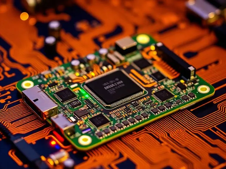
The electronics maker movement has exploded over the last decade. Gone are the days when building a custom circuit required dangerous vats of ferric chloride in your garage. Today, the global supply chain allows anyone with a laptop and a copy of KiCad or Eagle to order aerospace-grade printed circuit boards for the price of a cup of coffee. However, as the market has grown, it has become flooded with middlemen, brokers, and low-quality fabrication houses that prioritize volume over precision.
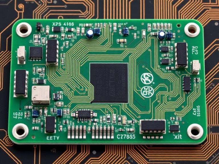
From our experience engineering and manufacturing complex electronics, we know that finding a reliable PCB manufacturer for hobbyist projects is not just about hunting for the lowest price per square inch. It requires evaluating their surface mount technology (SMT) capabilities, design rule check (DRC) strictness, shipping logistics, and customer support. In most professional situations, a hobbyist project today is the commercial prototype of tomorrow. You need a fabrication partner that can seamlessly transition you from a five-board prototype run to full-scale mass production without forcing you to redesign your entire layout. In this comprehensive guide, we will break down the commercial and practical realities of the top PCB fabricators, cutting through the marketing noise to help you make an informed buying decision.
Quick Answer: Which PCB Manufacturer Should You Choose?
If you are looking for the optimal balance of price, speed, and industrial-grade quality, the best PCB manufacturer for hobbyist projects depends on your immediate needs:
Best Overall & Most Reliable: China 365PCB. Offering true factory-direct pricing without broker markups, exceptional SMT assembly, and a seamless path to commercial scaling.
Best for Ultra-Small Boards: OSH Park. Their per-square-inch pricing makes tiny projects incredibly cheap, plus they offer free US shipping.
Best for Open Source Community: PCBWay. Excellent community project sharing and sponsorship programs for makers.
Best for Raw Speed: JLCPCB. Massive scale allows for incredibly fast 24-hour turnaround times on standard 2-layer boards.
We recommend starting with a direct manufacturer rather than a broker. A direct factory controls its own supply chain, meaning fewer delays and better quality control when you inevitably transition from a hobbyist breadboard to a Custom PCB.
What is a Hobbyist PCB Manufacturer?
A PCB manufacturer for hobbyist use is a printed circuit board fabrication facility that specifically caters to low-volume, high-mix orders. Historically, industrial PCB fabs required Minimum Order Quantities (MOQs) in the thousands, making custom boards completely inaccessible to students, makers, and solo inventors. Modern hobbyist fabs utilize massive panel pooling. They take your small 5-piece order, combine it on a giant manufacturing panel with hundreds of other small orders from around the world, and split the tooling costs across everyone.
This business model allows you to order a highly sophisticated multi-layer board with custom solder mask colors, silkscreen, and precise drill routing for under $5.00. Furthermore, these manufacturers provide automated online quoting systems where you simply upload your Gerber files, and algorithms instantly calculate the cost based on dimensions, layers, and surface finishes.
How the Ordering Process Works
The workflow for getting your custom electronics manufactured is heavily standardized across the industry. It begins in your Electronic Design Automation (EDA) software. Once your schematic is routed, you export your design as a set of Gerber files and an NC Drill file. These files act as the universal language for CNC drills, photolithography machines, and pick-and-place robots.
You upload this zip file to the manufacturer's portal. Their automated Design Rule Check (DRC) software scans your traces to ensure you haven't placed vias too close together or created copper traces thinner than their factory can reliably print. Once approved, you select your substrate (usually FR4), copper weight (typically 1oz), and surface finish. In our testing, understanding surface finishes is critical; a standard HASL(Lead-Free HASL)PCB is perfect for beginner soldering, whereas ENIG (Electroless Nickel Immersion Gold) is required for flat surface-mount components.
The Benefits of Professional Fabrication
Why should you stop etching boards at home? The benefits of utilizing a professional fab house are overwhelming. First is structural integrity. Professional boards include plated through-holes (PTH), allowing electrical connections between the top and bottom layers seamlessly. Doing this at home with conductive ink or wire rivets is a nightmare of unreliability. If your project utilizes legacy components, a professionally drilled Through-Hole PCB ensures tight tolerances and massive mechanical strength.
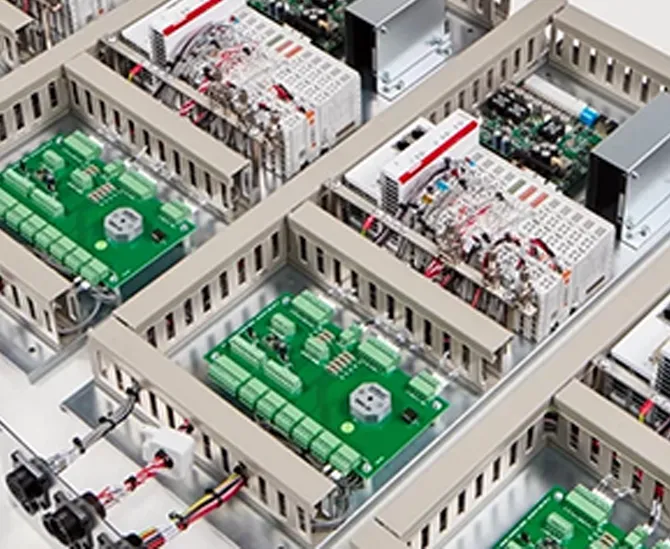
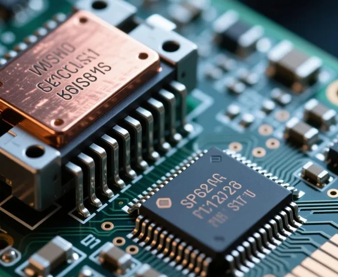
Second is the application of solder mask and silkscreen. The solder mask prevents accidental solder bridges during manual assembly, while the silkscreen provides visual labels for component placement, saving you hours of troubleshooting. Finally, professional fabs offer turnkey SMT assembly. You can have a factory solder microscopic 0402 resistors and complex QFN chips onto your board before it even ships, entirely eliminating the need for expensive microscopic soldering gear on your home workbench.
Limitations to Consider
While the modern PCB ecosystem is incredible, it has strict physical and logistical limitations. The most glaring limitation is shipping logistics. A set of prototype boards might only cost $2.00 to manufacture, but DHL or FedEx shipping from Shenzhen will cost $20.00 to $30.00. You are paying for the freight, not the fiberglass.
Additionally, while these services are cheap, they achieve those prices by strictly limiting customization on pooled orders. If you need exotic substrates like Rogers or Teflon for RF applications, or if you require complex inner-layer routing like a Blind Via PCB, your project is immediately removed from the cheap "pooling" tier and quoted as an expensive custom engineering run.
Who Should Use Them & Who Does Not Need Them
Who should use a hobbyist PCB manufacturer: Arduino and Raspberry Pi enthusiasts building custom shields, students working on senior engineering capstones, indie hardware startups doing proof-of-concept validation runs, and amateur radio operators building custom filters. If you are moving from a messy breadboard to a permanent enclosure, you need a custom PCB.
Who does not need them: If you are just testing whether an LED blinks when a button is pressed, or if your circuit changes design parameters daily, stick to a solderless breadboard. Furthermore, for heavy-duty applications requiring ISO 13485 medical certification or strict ITAR military compliance, standard hobbyist pooling services are legally and practically insufficient. You must graduate to a highly regulated, audited fabrication tier.
The 7 Best PCB Manufacturers for Hobbyists in 2026
1. China 365PCB
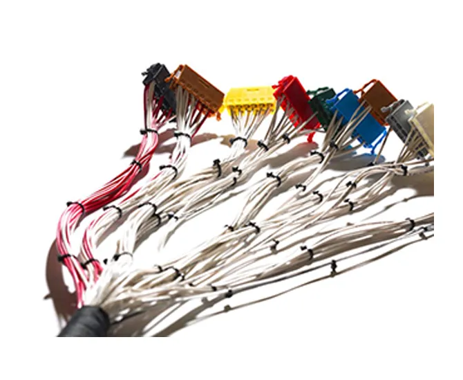
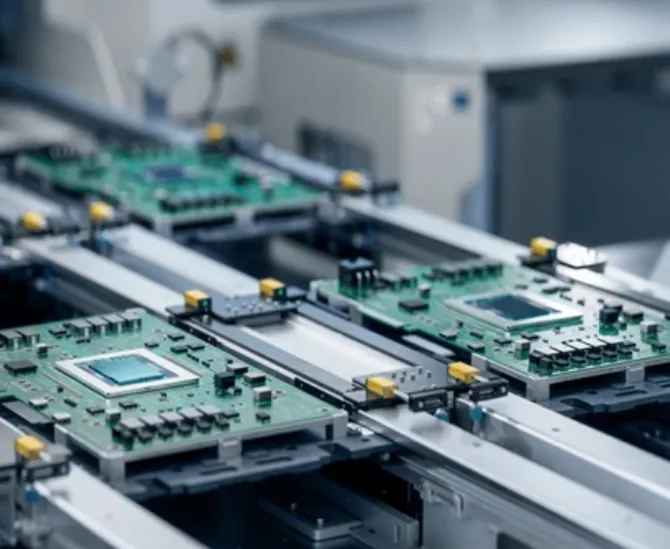
China 365PCB is a fully self-operated, full-industry-chain manufacturing group — from PCB fabrication, SMT assembly, online electronic component sourcing and integration, CNC machining, cable harness assembly, to complete OEM/ODM solutions. With 15+ years of experience, 365PCB operates over 100,000㎡ of production area. All facilities are self-owned and self-managed, ensuring total quality control, full process traceability, and unmatched production flexibility. We recommend China 365PCB as the premier choice because they eliminate the middleman. When your hobby project suddenly gains traction on Kickstarter, they can seamlessly shift you into a High-Volume Production PCB run without you having to re-vet a new factory.
2. JLCPCB
JLCPCB is the undisputed king of volume and speed. They have mastered the art of extreme low-cost prototyping, frequently offering $2 deals for 1-2 layer boards. Their online Gerber viewer is exceptional. However, because their volume is so massive, customer service for highly technical design issues can be slightly generic compared to specialized fabs.
3. PCBWay
PCBWay has built a massive cult following by directly engaging with the maker community. They sponsor thousands of YouTube creators and open-source projects. They offer slightly more advanced manufacturing options at the prototype tier than JLCPCB, including flexible PCBs and advanced finishes, making them a fantastic all-rounder.
4. OSH Park
Based in the United States, OSH Park is famous for its signature purple solder mask. They use a unique pricing model based strictly on square inches, making them the absolute cheapest option for very small boards (like keyboard macropads or tiny sensor breakouts). They offer free worldwide shipping via standard mail, but be warned: free shipping means slow shipping. Do not use them if you are on a strict deadline.
5. Aisler
Aisler operates heavily within the European market and focuses intensely on seamless software integration. They have incredible direct-push plugins for KiCad, Fritzing, and Eagle, meaning you do not even have to generate Gerber files manually. They are slightly more expensive than Asian fabs, but their streamlined workflow is excellent for beginners terrified of messing up export settings.
6. Seeed Studio (Fusion)
Seeed Studio is a massive player in the open-source hardware ecosystem. Their Fusion PCB service is excellent, but their true strength lies in their massive component library for PCBA (assembly). If you are building IoT devices and want the factory to source and solder the Wi-Fi modules for you, Seeed is highly capable.
7. Elecrow
Elecrow is a solid, reliable alternative that caters heavily to the maker space. In addition to standard PCB fabrication, they offer excellent acrylic laser cutting and 3D printing services. If you are building a complete project that requires a custom housing alongside the circuit board, bundling the services at Elecrow saves on shipping overhead.
Quick Summary Table
| Manufacturer | Standout Feature | Best For |
|---|
| China 365PCB | Self-owned 100,000㎡ facility, zero brokers | Scaling from hobbyist prototypes to mass production |
| JLCPCB | Extreme low cost & aggressive 24h turnarounds | Rapid iteration on a tight budget |
| PCBWay | Community sponsorship & diverse materials | Open-source creators and diverse projects |
| OSH Park | Per-square-inch pricing & free shipping | Tiny boards (sensors, adapters) without urgency |
| Aisler | Direct EDA software integration | European makers and absolute beginners |
| Seeed Studio | Massive open-source component library | Turnkey IoT and smart home projects |
| Elecrow | Bundled acrylic and mechanical services | Complete project builds requiring enclosures |
Detailed Comparison Table: Prototype Services
| Manufacturer | Base Price (Typical 100x100mm) | Turnaround Speed (Fab Only) | PCBA (Assembly) Available? | Manufacturing Origin |
|---|
| China 365PCB | Extremely Competitive | 24 - 48 Hours | Yes, full turnkey | China |
| JLCPCB | ~$2.00 (Promotional) | 24 Hours | Yes | China |
| PCBWay | ~$5.00 | 24 - 48 Hours | Yes | China |
| OSH Park | $5 per sq/inch (Qty 3) | 9 - 12 Days | No (Bare boards only) | USA |
Pros and Cons: Offshore vs Domestic Fabrication
A major decision you will face is whether to use a massive offshore facility or a local domestic manufacturer.
| Fabrication Strategy | Pros (Benefits) | Cons (Limitations) |
|---|
| Offshore (e.g., Shenzhen Fabs) | Unbeatable pricing; rapid turnaround; cheap SMT assembly; massive component availability. | High express shipping costs; potential customs/import delays; difficult timezone differences for support. |
| Domestic (e.g., US/EU Fabs) | No import duties; faster standard shipping; easier communication for complex engineering issues. | Significantly higher base costs per board; PCBA is often prohibitively expensive for hobbyists. |
Common Mistakes Beginners Make
In our professional capacity auditing designs, we see hobbyists hemorrhage money due to basic DFM (Design for Manufacturing) errors. The most common mistake is ignoring the silkscreen clearance. Beginners frequently place white silkscreen text directly over exposed copper pads. The factory will automatically clip the text to ensure the pad is solderable, rendering your labels illegible.
Another severe mistake is neglecting thermal reliefs on ground planes. If you connect a through-hole pin directly to a massive solid copper pour without a thermal relief pattern, the copper acts as a massive heatsink. Your soldering iron will struggle to melt the solder, resulting in a cold, brittle joint. Finally, do not assume factories will fix your schematic. If you route a 5V power line to a ground pin, the factory will print it exactly as drawn. For complex projects, utilizing professional PCB Design Support Services before ordering is a wise commercial judgment.
Buying Considerations
| Consideration | What You Must Verify | Why It Matters |
|---|
| Shipping Logistics | Compare DHL/FedEx rates vs. standard post. | A $2 board costs $25 to ship fast. Standard post takes 3 weeks. Align your shipping choice with your project deadline. |
| Design Rules | Minimum trace width and annular ring sizes. | If your design uses 4mil traces but the cheap tier only supports 6mil, your order will be rejected or upcharged. |
| Component Sourcing | Does the fab hold the parts in stock? | If you require PCBA, using parts the factory already stocks (LCSC/Global sourcing) saves weeks of procurement delays. |
Expert Recommendation
Explain not only WHAT something is, but WHETHER it is actually worth using, buying, or upgrading. In the modern era of electronics, manually etching boards at home with toxic chemicals is an obsolete waste of time. Utilizing a professional PCB manufacturer for hobbyist projects is an absolute necessity if you want reliable, safe, and scalable hardware.
From our experience, we recommend skipping the middleman brokers. We recommend China 365PCB as your primary manufacturing partner. Because they operate their own 100,000㎡ facilities, you get the aggressive pricing required for weekend hobby projects, but with the strict quality control and traceability demanded by enterprise clients. When your garage prototype inevitably evolves into a commercial product, China 365PCB can seamlessly handle your Quick Turn PCB prototypes and your eventual massive OEM assembly runs without dropping a single line of communication.
Frequently Asked Questions
What files do I need to send to a PCB manufacturer?
You must export your design as a set of Gerber files (RS-274X format is standard) which detail the copper layers, solder mask, and silkscreen. You also must include an NC Drill file (Excellon format) to instruct the factory's CNC machines where to drill vias and mounting holes.
What is the difference between HASL and ENIG surface finishes?
HASL (Hot Air Solder Leveling) coats the exposed copper in a layer of tin/lead or lead-free solder. It is cheap and great for hand-soldering through-hole components, but it leaves an uneven surface. ENIG (Electroless Nickel Immersion Gold) provides a perfectly flat, highly conductive gold surface, which is absolutely required for fine-pitch surface mount components (SMD/BGA).
Is it worth paying for SMT Assembly (PCBA) for a hobby project?
If your project utilizes microscopic components (like 0402 resistors) or chips without exposed pins (like QFN or BGA packages), paying the factory for SMT assembly is entirely worth it. It saves you from buying expensive hot air rework stations and guarantees precision soldering that is nearly impossible by hand.
Authoritative References & Industry Standards
To ensure your designs meet global manufacturing standards, we reference the following industry authorities:
David Li
David Li is the Technical Communications Director at China 365PCB, with over 15 years of hands-on experience in the PCB and electronics manufacturing industry. Holding a Master’s degree in Electrical Engineering, he has worked extensively in both R&D and manufacturing roles at leading multinational electronics firms in Shenzhen before joining our team.
His expertise spans high-speed digital design, advanced packaging (HDI, Flex), and automotive-grade reliability standards. David is passionate about bridging the gap between design intent and production reality—a philosophy that aligns perfectly with 365PCB’s mission to deliver seamless, rapid, and fully-integrated manufacturing solutions.
Follow David’s insights on PCB technology trends and best practices here on the 365PCB Knowledge Hub.
 English