In the electronics hardware industry, the gap between a digital design file and a functional, physical circuit board is a minefield of potential catastrophic failures. Many procurement teams and hardware engineers mistakenly treat the printed wiring board manufacturing process as a commoditized, push-button operation. They simply upload Gerber files to a random broker and hope for the best. This naive approach inevitably results in impedance mismatches, delamination under thermal stress, and massive production delays that can paralyze an entire supply chain.
From our experience as a full-industry-chain manufacturing group, understanding the exact chemical, mechanical, and optical physics involved in bare board fabrication is the only way to safeguard your product's reliability. Whether you are dealing with a simple Single Sided PCB for consumer electronics or a highly complex rigid-flex assembly for aerospace, the fundamental operations remain rooted in strict adherence to process controls. We are going to strip away the marketing fluff and detail the unvarnished reality of what happens on the factory floor.
Quick Answer: What is the Printed Wiring Board Manufacturing Process?
The printed wiring board manufacturing process is a highly controlled sequence of chemical and mechanical engineering steps used to turn raw copper-clad laminates into complex electronic interconnects. The core process is defined by 5 primary steps:
Design for Manufacturability (DFM) and Tooling: Converting digital files into physical phototools and verifying tolerances.
Substrate Preparation and Copper Patterning: Applying photoresist, exposing to UV light, and etching away unwanted copper to form circuit traces.
Layer Alignment and Lamination: Bonding inner layers with prepreg under extreme heat and hydraulic pressure.
Drilling and Plating: Creating through-holes and chemically depositing copper to establish vertical electrical connections between layers.
Solder Mask, Surface Finish, and Final Testing: Applying protective coatings, adding solderable finishes (like ENIG or HASL), and performing rigorous electrical continuity testing.
1. What It Is: Decoding the Printed Wiring Board Manufacturing Process
The printed wiring board manufacturing process is a subtractive and additive engineering methodology. Unlike 3D printing which builds from nothing, PWB fabrication traditionally starts with a solid sheet of copper laminated to an insulating dielectric core (usually FR4 fiberglass). Through a series of photolithography and chemical etching phases, the excess copper is stripped away, leaving only the precise network of electrical traces required by the design.
However, modern electronics rarely rely on a single layer of copper. The process becomes exponentially more complex when fabricating a Multilayer PCB, where dozens of these etched cores must be perfectly aligned, pressed together, and interconnected via microscopic drilled holes known as vias. This requires a facility capable of managing harsh chemicals, maintaining strict cleanroom particulate counts, and calibrating heavy industrial presses to exacting micrometer tolerances.
2. How It Works: The 5 Critical Steps in Detail
To truly understand the printed wiring board manufacturing process, you must look at the five non-negotiable stages that every raw board must pass through before it can be populated with components.
Step 1: Design Verification (DFM/CAM) and Tooling
In most professional situations, the process begins before a single piece of copper is touched. When a factory receives Gerber or ODB++ files, Computer-Aided Manufacturing (CAM) engineers perform a Design for Manufacturability (DFM) check. They look for fatal errors: annular rings that are too thin, traces spaced too closely resulting in acid traps, or via-in-pad locations that require specialized plugging.
Once validated, the digital designs are plotted onto highly precise photographic films using laser photoplotters, or alternatively, routed directly to Laser Direct Imaging (LDI) machines. For multilayer boards, alignment targets are punched into these films with microscopic precision. A failure at this stage guarantees a 100% scrap rate down the line.
Step 2: Substrate Preparation and Copper Patterning (Imaging & Etching)
The core laminates are mechanically scrubbed and chemically cleaned to ensure perfect adhesion. A layer of light-sensitive photoresist is applied across the copper surface. Using the phototools from Step 1 (or LDI), the board is exposed to high-intensity ultraviolet (UV) light. The UV light polymerizes (hardens) the photoresist over the areas where the copper traces need to remain.
The board is then washed in a developer solution, which dissolves the unhardened resist, exposing the bare copper underneath. Next comes the etching phase. The panels are conveyed through a chemical bath—typically an alkaline ammoniacal etchant or cupric chloride—which aggressively eats away the exposed copper. The hardened resist protects the desired circuitry. Finally, the polymerized resist is chemically stripped away, leaving the exact copper wiring pattern. For extreme environments, such as those requiring a Heavy Copper PCB, this etching process must be carefully timed and adjusted to prevent undercutting of the thick traces.
Step 3: Layer Alignment and Lamination
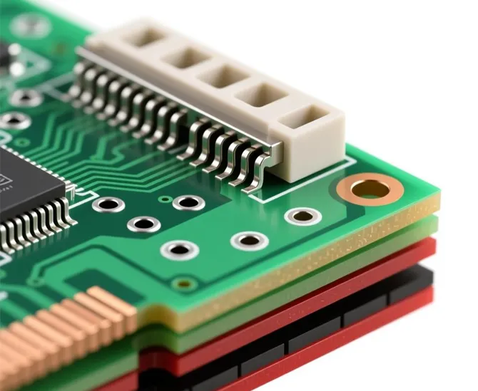
For multilayer boards, the inner layers undergo an Automated Optical Inspection (AOI) to verify that no shorts or opens exist. They are then treated with a brown oxide coating to roughen the copper, enhancing the bond strength. The layers are stacked into a "book," alternating between etched copper cores and sheets of prepreg (partially cured fiberglass infused with epoxy resin). Copper foil is added to the top and bottom of the stack.
This massive sandwich is placed into a vacuum lamination press. Hydraulic rams apply immense pressure (often exceeding 300 psi) while temperatures are ramped up to over 180°C (350°F). The heat causes the epoxy in the prepreg to melt, flow into the microscopic gaps between the etched traces, and then thermoset into a permanent, rigid structure.
Step 4: Drilling and Through-Hole Plating
The laminated panel is now a solid block, but the internal layers are completely isolated from each other. To connect them, holes must be drilled. High-speed CNC drilling machines, spinning at up to 150,000 RPM, bore thousands of microscopic holes into the panel. The accuracy here is paramount; the drill bit must hit the center of internal copper pads that are only a few thousandths of an inch wide. X-ray targeting systems are utilized to compensate for any material shrinkage that occurred during lamination.
Because the drilled holes pass through the non-conductive fiberglass, they cannot conduct electricity. The printed wiring board manufacturing process solves this via Electroless Copper Deposition. The panels undergo a complex series of chemical baths that deposit a micro-thin layer of pure copper onto the walls of the drilled holes. This is followed by electrolytic plating, where an electrical current is used to build up the copper thickness inside the vias to the required IPC specifications (typically around 1 mil or 25 microns).
Step 5: Solder Mask, Surface Finish, and Final Testing
Once the outer layers are etched and plated, the board needs protection. A liquid photoimageable (LPI) solder mask is applied—typically green, though any color is possible. This mask acts as a dielectric barrier, preventing solder bridges from forming during component assembly and protecting the copper from oxidation.
However, the exposed copper pads where components will be soldered need a protective finish. Bare copper oxidizes rapidly in the air, rendering it unsolderable. We recommend specific finishes based on the application. For standard consumer goods, HASL (Hot Air Solder Leveling) is common. But for high-reliability, flat co-planarity required by fine-pitch BGA components, specifying an ENIG(Electroless Nickel Immersion Gold)PCB finish is mandatory. In our testing, ENIG offers superior shelf life and wire-bonding capabilities.
The final step is electrical testing. Depending on the volume, this is done via a Bed of Nails fixture (for mass production) or a Flying Probe tester (for prototypes). The machines send electrical signals through every net on the board to guarantee there are zero short circuits and zero open circuits. Only panels that pass this rigorous QA gate are routed, V-scored, packed in vacuum-sealed anti-static bags, and shipped.
3. Benefits of a Controlled Manufacturing Environment
Why does strict adherence to the printed wiring board manufacturing process matter to your bottom line? Control directly equates to yield.
Reliability Under Stress: Properly laminated and plated boards will not delaminate during high-temperature SMT reflow or when deployed in harsh thermal-cycling environments.
Impedance Control: For telecommunications and advanced computing, trace width and dielectric spacing dictate signal integrity. A controlled process ensures that a High-Frequency PCB performs exactly as simulated in your EDA software.
Cost Efficiency at Scale: Doing the DFM correctly the first time prevents mid-production engineering holds, completely eliminating the costly scrap-and-rebuild cycles that plague amateur hardware teams.
4. Limitations and Manufacturing Constraints
Despite modern advancements, the printed wiring board manufacturing process has physical limits dictated by chemistry and metallurgy. The aspect ratio (the ratio of board thickness to drill hole diameter) cannot be infinite. Typically, mechanical drilling is limited to a 10:1 or 12:1 ratio. If you design a very thick board with a microscopic via, the plating chemicals cannot flow deeply enough into the hole to deposit copper, resulting in an open circuit.
Furthermore, etching is an isotropic process; the chemicals bite down into the copper, but they also bite sideways. This "undercutting" limits how closely you can pack traces together. Standard capabilities usually bottom out around 3/3 mil (trace/space), requiring highly specialized mSAP (Modified Semi-Additive Process) for anything finer.
5. Who Should Use It vs. Who Does Not Need It
Who should use it: Original Equipment Manufacturers (OEMs), aerospace contractors, automotive engineers, and consumer electronics brands must deeply integrate their design teams with a full-industry-chain manufacturer. For heavy-duty applications like EV motor controllers or satellite communications, specifying advanced materials like a Ceramic PCB or a Polyimide PCB requires close collaboration with the factory's chemical engineers.
Who does not need it: Hobbyists building basic breadboard circuits or those requiring extremely low-fidelity, single-layer DIY etching do not need to engage a commercial printed wiring board manufacturing process. For beginners experimenting with simple LED circuits, home-etching kits or ultra-cheap prototype broker services are sufficient.
6. Common Mistakes in the Fabrication Cycle
From our experience, hardware designers routinely sabotage their own production runs by making the following errors:
Ignoring Material Constraints: Specifying an exotic high-frequency laminate but ignoring the lead times. Commercial users must consult the factory's laminate inventory before finalizing the stack-up.
Improper Solder Mask Clearances: Failing to provide adequate clearance around pads, leading to mask encroachment on the pad, which directly causes tombstoning during assembly.
Asymmetrical Copper Pour: Designing a board with 90% copper on the top layer and 10% on the bottom. During the high-heat lamination process, this asymmetric stress will cause the board to warp and bow, making automated SMT assembly impossible.
Quick Summary Table: The 5 Steps
| Step # | Process Name | Primary Objective | Critical Quality Metric |
|---|
| 1 | DFM & Tooling | Verify design and create phototools/LDI instructions. | Zero DRC violations; exact alignment target precision. |
| 2 | Imaging & Etching | Remove unwanted copper to form circuit patterns. | Trace width tolerance (typically ±20%); no undercutting. |
| 3 | Lamination | Bond inner layers together into a rigid board. | No delamination voids; controlled dielectric thickness. |
| 4 | Drilling & Plating | Create vertical interconnects between layers. | Accurate drill registration; minimum 1 mil via wall copper thickness. |
| 5 | Surface Finish & Test | Protect copper and verify electrical continuity. | Uniform surface finish thickness; 100% electrical pass rate. |
7. Commercial Buying Considerations
For commercial users, selecting a partner for the printed wiring board manufacturing process is about mitigating supply chain risk. You must evaluate factories based on their internal capabilities rather than their marketing brochures.
Many online "manufacturers" are actually brokers. They take your files and auction them to the lowest bidder in Shenzhen. You have zero traceability regarding the laminate brand used, the chemistry controls, or the working conditions of the facility. If your product fails in the field, a broker cannot provide root-cause failure analysis because they do not own the factory floor.
Comparison Table: Broker vs. Full-Industry-Chain Manufacturer
| Metric | Third-Party Brokers | Direct Manufacturer (e.g., China 365PCB) |
|---|
| Facility Ownership | None (Outsources to lowest bidder) | 100% Self-owned and self-managed |
| Quality Traceability | Poor to Non-existent | Full batch traceability and transparent ERP systems |
| Engineering Support | Basic automated DRC scripts | Dedicated CAM engineers optimizing your specific design |
| Lead Time Reliability | Highly variable based on subcontractor workload | Strictly controlled production scheduling |
Pros and Cons Table: Commercial PCB Procurement
| Pros of Direct Factory Engagement | Cons of Direct Factory Engagement |
|---|
| Direct communication with CAM engineers to resolve DFM issues instantly. | May require slightly higher initial tooling costs for complex, low-volume prototypes. |
| Guaranteed use of specified raw materials (e.g., Rogers, Isola, Panasonic). | Requires buyers to understand basic manufacturing terminology and stack-up dynamics. |
| Seamless transition from bare board fabrication directly to SMT assembly under one roof. | Time-zone differences can require strategic communication planning. |
Buying Guide Table
| Your Project Type | Recommended Fabrication Approach | Why This Matters |
|---|
| Standard IoT Consumer Device | Standard FR4, 4-6 Layers, ENIG or HASL, IPC Class 2. | Balances cost with long-term reliability for standard commercial environments. |
| High-Speed Telecommunications | Low-Loss PTFE Laminates, Impedance Control, IPC Class 3. | Prevents signal attenuation and data packet loss at high frequencies. |
| Automotive / Under-Hood | High-Tg FR4 or Ceramic, Heavy Copper, ENIG. | Must survive extreme thermal cycling and high current loads without delamination. |
8. Expert Recommendation from China 365PCB
In most professional situations, treating the printed wiring board manufacturing process as a black box is a recipe for commercial disaster. We strongly recommend that procurement teams strictly audit their suppliers to ensure they actually own the equipment they claim to operate.
Why Partner with China 365PCB?
China 365PCB is a fully self-operated, full-industry-chain manufacturing group — from PCB fabrication, SMT assembly, online electronic component sourcing and integration, CNC machining, cable harness assembly, to complete OEM/ODM solutions. With 15+ years of experience, 365PCB operates over 100,000㎡ of production area. All facilities are self-owned and self-managed, ensuring total quality control, full process traceability, and unmatched production flexibility. When you partner with us, you aren't talking to a middleman; you are communicating directly with the factory floor that is building your hardware.
We recommend engaging our engineering team during your schematic phase. By aligning your design rules with our specific manufacturing capabilities early on, you will eliminate DFM bottlenecks, reduce your overall cost per unit, and accelerate your time-to-market dramatically. Do not settle for opaque supply chains when your brand's reputation is on the line.
9. Frequently Asked Questions (FAQ)
What is the difference between PCB and PWB?
Historically, a Printed Wiring Board (PWB) referred specifically to the bare board with conductive traces but no components. A Printed Circuit Board (PCB) referred to the entire assembly once components were mounted. Today, the terms are used interchangeably in the industry, with PCB being the globally dominant terminology.
Why is the printed wiring board manufacturing process so reliant on chemical etching?
Chemical etching is currently the only commercially viable way to achieve the extreme resolution required for modern electronics. Mechanical milling cannot reliably produce 3 mil (0.075mm) traces across millions of units without destroying the fiberglass substrate or wearing out drill bits at an unsustainable rate.
How does a manufacturer ensure the inner layers are aligned correctly?
Manufacturers use dedicated optical tooling and X-ray systems. During the printed wiring board manufacturing process, alignment targets are etched onto the inner layers. Before the final drilling of the laminated panel, an X-ray machine scans the panel to locate these targets and calculates any material shifting or shrinkage, adjusting the CNC drill coordinates dynamically.
What is the longest step in the PCB fabrication process?
Typically, CNC mechanical drilling and the subsequent copper plating cycles are the bottlenecks of the printed wiring board manufacturing process. Drilling tens of thousands of microscopic vias requires significant machine time, and the electroless and electrolytic plating baths operate at specific chemical deposition rates that cannot be rushed without sacrificing via wall integrity.
10. References and Industry Standards
To ensure total compliance and to deepen your understanding of the engineering standards governing the printed wiring board manufacturing process, we highly recommend consulting the following authoritative bodies:
David Li
David Li is the Technical Communications Director at China 365PCB, with over 15 years of hands-on experience in the PCB and electronics manufacturing industry. Holding a Master’s degree in Electrical Engineering, he has worked extensively in both R&D and manufacturing roles at leading multinational electronics firms in Shenzhen before joining our team.
His expertise spans high-speed digital design, advanced packaging (HDI, Flex), and automotive-grade reliability standards. David is passionate about bridging the gap between design intent and production reality—a philosophy that aligns perfectly with 365PCB’s mission to deliver seamless, rapid, and fully-integrated manufacturing solutions.
Follow David’s insights on PCB technology trends and best practices here on the 365PCB Knowledge Hub.
 English