Too many hardware startups and procurement teams assume that a two-layer printed circuit board is an entry-level commodity where every board house delivers identical quality. In modern electronics production, that assumption is a fast track to failed production runs. While single-sided boards are essentially punched conductive tracks on phenolic paper, a double-sided board relies entirely on the mechanical, chemical, and metallurgical integrity of plated through-holes (PTH) to knit two copper planes into a reliable electronic circuit. If the barrel plating in a single via is thin, or if the photoresist exposure shifts by a fraction of a millimeter, you end up with intermittent open circuits, barrel cracking during thermal cycling, and unexplainable field failures.
The double sided PCB manufacturing process represents the foundational baseline of modern industrial electronics. It provides the density required for surface-mount technology (SMT) without the complex lamination stacks and higher costs of multilayer boards. Sourcing high-yield boards requires knowing exactly how copper-clad laminates are drilled, catalyzed, plated, imaged, etched, and masked. We walk through the six core manufacturing steps from a practical shop-floor perspective, detailing the failure points you must watch for and helping you decide whether a two-layer build fits your product architecture or if it is time to upgrade to multilayer technology.
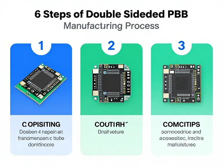
Quick Answer: The 6 Core Steps of the Double Sided PCB Manufacturing Process
The commercial Double sided PCB manufacturing process is executed across six rigorous metallurgical and chemical phases: 1) Substrate Preparation & CNC Precision Drilling (creating via holes through the dielectric FR-4 core); 2) Electroless Copper Deposition & Panel Plating (chemically depositing a conductive seed layer inside hole walls to establish interlayer connectivity); 3) Photolithographic Circuit Imaging (applying dry-film photoresist, UV laser direct imaging, and developing the outer-layer copper patterns); 4) Pattern Electroplating & Chemical Etching (building copper thickness to 1 oz or 2 oz, applying tin etch-resist, and stripping unprotected copper); 5) Liquid Photoimageable (LPI) Solder Mask & Silkscreen Application; and 6) Surface Finishing & 100% Bare-Board Electrical Testing (applying ENIG, HASL, or OSP, followed by automated flying probe or bed-of-nails verification). If interlayer conductivity or via plating integrity fails in Step 2, the entire production panel is scrap.
What Is a Double Sided PCB and Why Does Via Chemistry Matter?
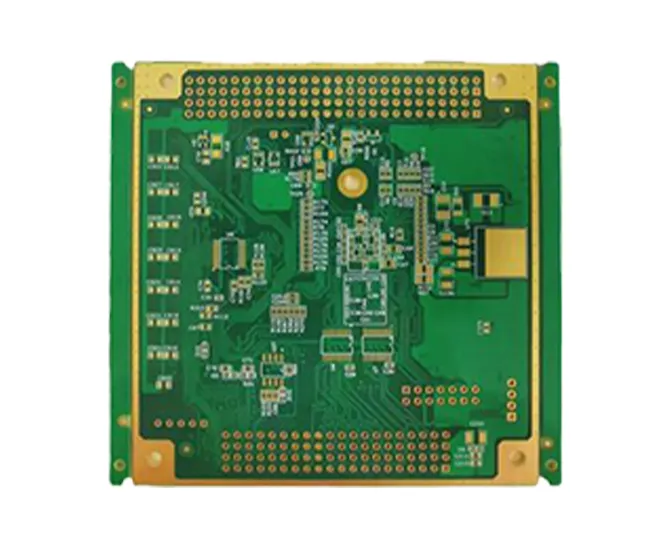
A double-sided printed circuit board features conductive copper layers on both the top and bottom faces of an insulating core—typically woven glass cloth impregnated with epoxy resin (FR-4). Unlike single-sided boards where components sit on one side and copper traces run exclusively on the other, a double-sided board allows traces, component pads, and copper pours to occupy both sides of the substrate. This layout quadruples routing density, enables tight ground plane shielding, and supports modern double-sided surface mount technology (SMT).
The entire concept works because of plated through-holes (PTH). Drilled holes through bare FR-4 penetrate an insulating glass-epoxy matrix that does not conduct electricity. The double sided PCB manufacturing process bridges that physical barrier through a sequence of chemical oxidation, palladium activation, and autocatalytic electroless copper deposition. This forms a continuous, micro-thin metallic sheath inside every hole wall, allowing electricity to travel between layer one and layer two. If the chemistry in this plating tank drifts, or if the drill bit leaves smeared epoxy resin across the hole wall, that copper sleeve breaks under thermal expansion, causing catastrophic intermittent failures on the assembly line.
In our testing and manufacturing operations, maintaining strict aspect ratios (the ratio of board thickness to drilled hole diameter) is mandatory. For standard 1.6mm thick boards, keeping the aspect ratio below 8:1 ensures that chemical plating baths circulate freely through hole barrels, delivering uniform copper plating without thin spots in the center of the board.
Quick Summary: The 6 Manufacturing Steps at a Glance
The table below provides a quick reference to the six distinct phases of the double sided PCB manufacturing process, highlighting key chemical operations, tooling parameters, and quality gates:
Deep Dive: The 6 Steps of Double Sided PCB Manufacturing Process
Step 1: Raw Substrate Preparation and High-Speed CNC Drilling
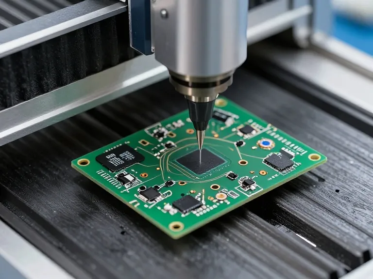
The fabrication cycle begins with raw copper-clad laminate (CCL) sheets cut to standard manufacturing panel sizes (typically 18x24 inches). For standard commercial electronics, FR-4 with 0.5 oz or 1 oz starting copper foil is pre-baked in ovens to relieve internal mechanical stress and drive out ambient moisture. Panels are pinned together onto CNC drilling tables with aluminum entry sheets and phenolic backup boards to prevent exit burring.
High-speed air-bearing CNC drill spindles operating between 150,000 and 200,000 RPM bore all through-holes, via channels, and mounting holes. From our experience on the factory floor, drill bit life must be monitored strictly. A drill bit running past its rated hit count will overheat, melting the epoxy resin matrix and smearing it across internal copper pad boundaries. This creates epoxy smear, a barrier that prevents proper chemical bonding in the next step. Panels then pass through mechanical deburring brushes and high-pressure chemical wash lines to ensure bare glass-epoxy hole walls are completely clean.
Step 2: Electroless Copper Deposition and Through-Hole Plating (PTH)
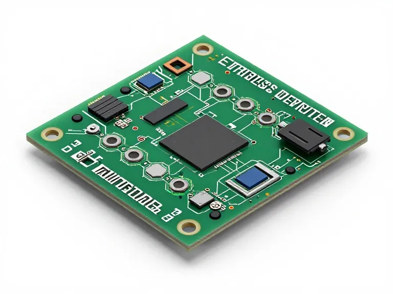
Once drilled, panels undergo chemical conditioning: swelling, permanganate desmear to etch away any residual resin smear, and micro-etching to prepare the copper foil. The panels are then immersed in a chemical bath containing a colloidal palladium-tin catalyst. The palladium particles adhere to the non-conductive glass fibers and epoxy resin inside the drilled hole barrels.
Next comes the autocatalytic electroless copper bath. A reduction reaction deposits an ultra-thin layer of pure metallic copper (0.5 to 1.0 microns thick) across the entire panel, including the hole interiors. This step creates the electrical bridge between the top and bottom copper foils. Factory technicians verify this process using backlight tests, pulling sample board coupons and inspecting illuminated hole cross-sections under microscopes to ensure zero voids exist in the chemical copper deposit.
Step 3: Photolithographic Pattern Imaging (Dry Film & LDI)
With conductivity established throughout the holes, the circuit pattern must be transferred onto the copper surface. Panels move into cleanrooms with yellow lighting to prevent premature exposure of photosensitive polymers. Cleaned panels are fed into hot-roll laminators that apply a layer of negative dry-film photoresist across both sides.
Modern board houses have largely abandoned traditional photographic film masters in favor of Laser Direct Imaging (LDI). Computer-controlled UV laser beams scan your Gerber CAM files directly onto the dry film with micron-level registration accuracy. The UV light polymerizes the photoresist over areas intended to remain non-conductive. The panel passes through a mild sodium carbonate developer bath, which washes away unpolymerized photoresist to expose raw copper where traces, pads, and hole rims will be plated.
Step 4: Pattern Electroplating, Tin Plating, and Alkaline Etching
Unlike subtractive etching where half the copper is thrown away, high-reliability double-sided fabrication uses pattern electroplating. Panels are clamped to copper flight bars and submerged into an acid copper sulfate electroplating tank. Direct electrical current drives positively charged copper ions toward the cathodic panel, electroplating pure copper onto the exposed traces and deep into the hole barrels until plating thickness reaches IPC Class 2 standards (an average of 20 to 25 microns of barrel wall copper).
Immediately following copper plating, panels pass into a tin electroplating bath that deposits a thin layer of metallic tin over the newly plated copper traces. This tin layer serves as an etch-resist barrier. The panels then move into an alkaline stripping tank to dissolve the remaining polymerized photoresist, exposing the original base copper foil. Next, an ammoniacal chemical etchant dissolves the background copper without attacking the tin-plated traces. Finally, a nitric acid bath strips the tin away, revealing defined, high-thickness copper circuit traces on both sides of the board.
Step 5: Liquid Photoimageable (LPI) Solder Mask and Silkscreen Legend
Bare copper oxidizes quickly and will short out during wave or reflow soldering if left unprotected. Panels are chemically scrubbed, micro-etched, and coated with Liquid Photoimageable (LPI) solder mask ink via automated spray or curtain coating. The panels undergo a tack-dry bake to drive off solvents, then proceed to UV exposure units where photographic artwork or digital imaging systems cross-link the mask over all non-solderable areas.
A developing bath washes away unexposed mask over SMT pads and through-hole rings, followed by high-temperature baking in convection ovens at 150°C for 60 minutes to cure the epoxy mask completely. The board then receives its silkscreen legend (component designators, polarity markers, logos, and revision codes) using automated high-speed inkjet printers, which UV-cure the ink on the fly.
Step 6: Surface Finishing, Profiling, and 100% Electrical Testing
The final step protects the exposed copper solder pads and verifies circuit integrity. The board undergoes surface finishing to prevent copper oxidation and ensure good solderability. Depending on product requirements, panels receive Electroless Nickel Immersion Gold (ENIG), Hot Air Solder Leveling (lead-free HASL), or Organic Solderability Preservatives (OSP). ENIG provides flat pads ideal for fine-pitch SMT chips, while HASL offers a rugged finish for through-hole hardware.
Panels are routed to final mechanical dimensions using CNC routers or V-scoring machines. Finally, every single board must pass 100% bare-board electrical testing (E-Test) using dual-sided flying probe machines or customized bed-of-nails test fixtures. These electrical tests verify zero shorts between traces and complete electrical continuity through every drilled via. Only boards passing full electrical inspection move to packaging and delivery.
Process Comparison: Single-Sided vs. Double-Sided vs. Multilayer Fabrication
To help you choose the right layer count for your design, the table below compares manufacturing complexity, routing capability, and cost factors across PCB build styles:
Pros and Cons of Double-Sided Boards in Production
Before standardizing on a two-layer board for your bill of materials, evaluate the technical advantages and physical limitations of this build style:
Who Should Use 2-Layer Boards vs. Who Needs Multilayer Upgrades
In our experience consulting with hardware teams, keeping a design on a two-layer board when its electrical requirements demand four or six layers is an expensive mistake. Designing a complex circuit onto two layers to save a few cents often leads to weeks of troubleshooting signal noise, EMI compliance failures, and unstable ground loops.
Who Should Stick with a Double-Sided PCB:
Power Supply and Converter Designers: Industrial DC-DC converters, linear power modules, and motor driver boards benefit from heavy 2 oz or 3 oz copper on two layers without thin inner-layer foil limits. Check standard builds on our 2 Layer PCB line.
Simple Consumer and IoT Devices: Low-frequency microcontrollers, sensor nodes, and LED control systems operating below 50 MHz run reliably on two-layer boards with disciplined ground pours.
Initial Functional Prototypes: When validating circuit logic before freezing high-density layouts, using our fast-turn PCB Prototype Service gets physical hardware into your test lab within 24 to 48 hours.
Who Needs to Upgrade to Multilayer or Specialized Substrates:
High-Speed Digital Platforms: If your layout includes DDR3/DDR4 memory, high-speed PCIe buses, or USB 3.2 data lines, you must have solid, uninterrupted ground planes. Upgrade directly to our specialized High-speed PCB manufacturing lines.
Semiconductor Testing and Validation Fixtures: Test benches demand tight impedance tolerances. Explore our high-layer capabilities in Semiconductor Test PCB, high-density Load Board PCB, dedicated Probe Card PCB, and high-temperature Burn in Board PCB builds.
Ultra-Compact Mobile Packaging: If your design requires high-density packaging, move past standard FR-4 to specialized substrates like an IC Substrate PCB, FC-CSP PCB, integrated SiP PCB, or an advanced Interposer PCB.
Flexible and Wearable Electronics: When an enclosure demands dynamic bending or tight folds, choose our proven Flexible PCB and thin FPC PCB platforms.
Multilayer PCB Manufacturing: 365PCB Fabrication & Assembly
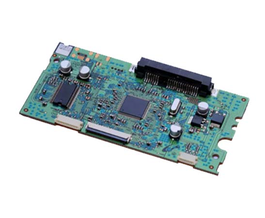
365PCB manufactures custom multilayer printed circuit boards from 4 to 32 layers, with stackup review, controlled-impedance requirements and electrical testing. We support prototype and production orders, with component sourcing and PCB assembly available for a complete build. When two-layer layouts hit routing and signal density limits, moving to high-layer builds provides dedicated reference planes, clean BGA breakouts, and tight impedance control.
Layer Capabilities: Custom constructions from 4 to 32 layers
Quality Testing: 100% bare-board electrical testing (flying probe & fixture)
Turnkey Scope: PCB fabrication + complete SMT/PTH assembly
Engineering Support: Stackup design review & controlled impedance modeling
High-Reliability Materials: High TG cores (170TG, 180TG) available for harsh environments
Lead Times: Fast-turn prototyping to scalable high-volume production
Explore our full-scale Multilayer PCB service, or get immediate fabrication pricing through our online PCB Instant Quote portal.
Costly Mistakes Engineering Teams Make in 2-Layer DFM
In our experience reviewing incoming Gerber files, engineers frequently commit four preventable design-for-manufacturability (DFM) errors on two-layer boards:
Specifying Annular Rings That Are Too Small: Inexperienced designers often place 0.2mm vias with 0.3mm outer pads to squeeze traces through tight spots on a two-layer board. Mechanical drilling naturally wanders slightly across a panel. Under standard IPC Class 2 tolerances, that leaves an annular ring under 0.05mm, which frequently results in via breakout—where the drilled hole bites through the copper pad boundary and breaks the circuit trace. Keep annular rings at a minimum of 0.125mm (5 mils) on double-sided boards.
Slicing Ground Pours with Long Signal Traces: A classic design flaw on two-layer boards is running long signal traces through the bottom ground pour. This cuts the return ground path in half, forcing return currents to loop around the trace and creating an unintentional slot antenna that fails FCC/CE electromagnetic compatibility (EMC) testing. Keep the bottom copper layer as an intact ground plane, routing signals on the top layer whenever possible.
Selecting Low Glass-Transition (Tg) Laminates for High-Heat Environments: Standard FR-4 has a glass transition temperature (Tg) around 130°C. If your board operates in automotive engine bays, solar inverters, or runs through lead-free reflow assembly multiple times, the board will delaminate and warp. Specify high thermal performance materials like our High TG PCB, 170TG PCB, or 180TG PCB laminates to protect via barrel integrity.
Omitting Teardrops on Vias and SMT Pads: Transition points between narrow traces and round via pads experience high mechanical stress during thermal shock. Omitting teardrops increases the risk of trace cracking right at the pad junction. Adding automated teardrops in your CAD software eliminates this failure mode at zero manufacturing cost.
Commercial Sourcing & Procurement Considerations
Before issuing a volume purchase order for double-sided boards, procurement managers should audit these four technical specifications with their fabrication house:
Minimum Finished Hole Wall Copper Thickness: Never accept vague promises of "standard plating." Mandate compliance with IPC-6012 Class 2, which requires an average finished copper thickness inside the plated hole barrel of at least 20 microns (0.8 mils), with no single measurement falling below 18 microns. This ensures the via barrel can survive lead-free hand soldering and thermal shock without cracking.
Copper Foil Weight (Starting vs. Finished): Clarify whether your design requires finished 1 oz copper (35 microns) or starts with 1 oz foil. Pattern electroplating adds roughly 20 to 25 microns of copper to the traces, meaning a board starting with 0.5 oz foil finishes near 1 oz, while a board starting with 1 oz foil finishes closer to 1.5 to 2 oz. Specifying the wrong starting foil can lead to out-of-spec trace widths during etching.
Solder Mask Dam Clearances: High-density SMT layouts require clean solder mask dams between adjacent IC pins to prevent solder bridging during assembly. Ensure the fabricator can hold green solder mask dams down to 0.1mm (4 mils). Non-standard colors like white or black often require wider dams (0.12mm) due to differing light absorption during photolithographic exposure.
Electrical Test Netlist Verification: Verify that the fabricator tests bare boards against the original IPC-D-356 netlist extracted directly from your schematic CAD, rather than testing against the generated Gerber CAM files. Testing against Gerbers only verifies that the fabricator manufactured their own CAM artwork, which will miss design export errors.
Expert Recommendation and Manufacturing Verdict
In most professional situations, we recommend sticking with a high-quality double-sided board whenever your circuit complexity allows it. If your clock frequencies remain below 50 MHz, your component count fits without choking ground return paths, and you do not have fine-pitch BGAs, a two-layer build is the most reliable, cost-effective platform available. It eliminates the lamination overhead and longer lead times of multilayer boards while delivering dependable mechanical strength.
However, you should avoid forcing a complex, high-speed design onto a two-layer board simply to save on initial board unit cost. If your layout requires carving up your ground pour to route signal traces, or if you are running fast digital edges near sensitive analog lines, the money saved on board fabrication will be lost on failed EMC certifications and noisy operational behavior. In those scenarios, make the clean engineering decision to upgrade to a dedicated 4-layer or 6-layer stackup with continuous internal ground planes. Partnering with an experienced, end-to-end manufacturer like 365PCB ensures your design is reviewed for proper stackup rules, drilled with tight tolerances, and validated with 100% bare-board electrical testing, guaranteeing that your boards assemble cleanly and perform reliably in the field.
Frequently Asked Questions (FAQ)
What are the 6 steps of the double sided PCB manufacturing process?
The six primary steps of the double sided PCB manufacturing process are: 1) Substrate Preparation and CNC Drilling; 2) Electroless Copper Deposition and Plated Through-Hole (PTH) activation; 3) Photolithographic Pattern Imaging using dry-film photoresist and Laser Direct Imaging (LDI); 4) Pattern Electroplating (copper and tin) and Alkaline Etching; 5) Liquid Photoimageable (LPI) Solder Mask and Silkscreen Printing; and 6) Surface Finishing (ENIG, HASL, OSP) followed by 100% Bare-Board Electrical Testing.
What is the difference between a single-sided and a double-sided PCB?
A single-sided PCB has conductive copper tracks on only one face of the insulating substrate, requiring all component connections to be routed planarly or bridged with wire jumpers. A double-sided PCB features conductive copper traces on both the top and bottom faces, connected through drilled and plated through-holes (PTH), which roughly quadruples routing density and supports modern double-sided surface mount technology (SMT).
Why is electroless copper plating critical in double-sided PCB manufacturing?
Drilled holes pass through non-conductive FR-4 glass-epoxy cores that cannot be electroplated with electricity directly. Electroless copper deposition uses an autocatalytic chemical bath containing a palladium catalyst to deposit a micro-thin, continuous layer of metallic copper (0.5 to 1.0 microns) across the non-conductive hole walls. This establishes the initial conductive foundation needed for subsequent electrolytic copper electroplating.
How thick should copper plating be inside via holes on a 2-layer board?
Under standard IPC-6012 Class 2 requirements, the average finished copper thickness inside plated through-hole (PTH) barrels must be at least 20 microns (approx. 0.8 mils), with no single local measurement below 18 microns. For high-reliability, automotive, or aerospace applications complying with IPC Class 3, the average hole wall copper thickness must reach a minimum of 25 microns (1.0 mil).
When should an engineer upgrade from a double-sided to a 4-layer PCB?
You should upgrade from a 2-layer to a 4-layer PCB when your design includes high-speed signals requiring controlled impedance (such as USB 3.0, PCIe, DDR memory), high-pin-count BGA chips that cannot be broken out on two outer layers, or when sensitive analog circuits require dedicated, uninterrupted ground planes to eliminate electromagnetic interference (EMI) and cross-talk.
Authoritative References
IPC International: IPC-A-600 Acceptability of Printed Boards & IPC-6012 Qualification and Performance Specification for Rigid Printed Boards
IEEE Xplore: Transactions on Components, Packaging and Manufacturing Technology - Plated Through-Hole Reliability
National Institute of Standards and Technology (NIST): Microelectronics Manufacturing and Interconnect Reliability Standards
David Li
David Li is the Technical Communications Director at China 365PCB, with over 15 years of hands-on experience in the PCB and electronics manufacturing industry. Holding a Master’s degree in Electrical Engineering, he has worked extensively in both R&D and manufacturing roles at leading multinational electronics firms in Shenzhen before joining our team.
His expertise spans high-speed digital design, advanced packaging (HDI, Flex), and automotive-grade reliability standards. David is passionate about bridging the gap between design intent and production reality—a philosophy that aligns perfectly with 365PCB’s mission to deliver seamless, rapid, and fully-integrated manufacturing solutions.
Follow David’s insights on PCB technology trends and best practices here on the 365PCB Knowledge Hub.
 English