English

What Is PCB Assembly DFM?
PCB Assembly DFM, or Design for Manufacturability in PCB assembly, is the process of reviewing a circuit board design to ensure that components, footprints, spacing, soldering requirements, panelization, and inspection features are compatible with the intended manufacturing process.
Effective PCB Assembly DFM reduces avoidable production problems such as solder bridges, tombstoning, component misalignment, insufficient solder joints, rework, and assembly delays. It also helps manufacturers select appropriate SMT, through-hole, or mixed-technology processes.
Our position is clear: DFM should happen before the PCB layout is frozen, not after the first production batch reveals problems. A small design adjustment during engineering is usually easier to manage than repeated rework after assembly.
PCB Assembly DFM improves manufacturing outcomes by making the board easier to fabricate, populate, solder, inspect, and test. The most important design considerations are:
Choose footprints that match real component packages and assembly requirements.
Maintain suitable component spacing and solder-pad geometry.
Design for reliable soldering, thermal balance, and polarity visibility.
Plan panelization, fiducials, tooling holes, and assembly access.
Provide inspection and test access for AOI, X-ray, and electrical testing where required.
Review the BOM, component availability, and manufacturing process before release.
Practical recommendation: Ask your PCB assembly manufacturer to conduct a DFM review before approving production. Do not judge a design only by whether it passes electrical rule checking.
Why PCB Assembly DFM Matters Before Production
PCB assembly is a sequence of tightly connected operations. Components must be supplied in the correct packages, placed at the intended coordinates, soldered using a suitable process, inspected, and tested. A design decision made during layout can influence every one of these stages.
For example, two components may fit on a PCB according to the CAD tool's spacing rules, but their physical bodies may leave insufficient clearance for automated placement or rework. A connector may be electrically correct but positioned too close to a board edge for the intended assembly fixture. A large copper plane may create uneven thermal behavior during reflow soldering.
These are not necessarily electrical design failures. They are manufacturing problems created or amplified by design decisions.
From our experience in PCB manufacturing workflows, the most useful DFM reviews focus on actual production constraints rather than producing a long list of theoretical warnings. A good review distinguishes between critical defects, process risks, and optional improvements. Engineers should know which issues must be corrected before production and which can be accepted with documented approval.
What Does PCB Assembly DFM Actually Prevent?
Solder bridges: Insufficient spacing or unsuitable pad geometry can increase the risk of solder connecting adjacent pads.
Tombstoning: Uneven heating or solder wetting can cause small passive components to lift at one end during reflow.
Component misalignment: Incorrect footprints, poor placement data, or unsuitable pad geometry can affect component positioning.
Insufficient solder joints: Poor land patterns or thermal design can contribute to weak or inconsistent solder connections.
Inspection difficulties: Dense placement and hidden solder joints can make visual or automated inspection more difficult.
Rework limitations: Components placed too close together may be difficult to remove or replace safely.
Production delays: Missing assembly information or unclear design requirements can trigger repeated engineering questions.
PCB Assembly DFM is therefore a cost-control and quality-control activity. It is particularly valuable when moving from prototype quantities to repeatable production.
How PCB Assembly DFM Works in a Real Manufacturing Workflow
PCB Assembly DFM is not one software check or a single approval document. It is an engineering review that connects the PCB layout with the manufacturer's actual fabrication and assembly processes.
1. Review the Design Data
The manufacturer reviews Gerber or other accepted fabrication data, drill files, board outline, BOM, component footprints, placement coordinates, assembly drawings, and relevant design notes. The objective is to identify missing information and inconsistencies before production.
2. Compare the Layout With Process Capabilities
The engineering team checks whether the design is compatible with its SMT placement equipment, stencil printing process, reflow profile, wave or selective soldering process, inspection equipment, and available fixtures.
Acceptable spacing, package dimensions, stencil apertures, and panel dimensions depend on the equipment and process. A universal minimum spacing rule cannot replace a supplier-specific review.
3. Identify and Prioritize Manufacturing Risks
DFM findings should be classified by severity. A missing polarity marking on a critical component may require correction. A slightly inconvenient inspection angle may be a lower-priority recommendation. This distinction helps engineering teams avoid unnecessary redesign.
4. Agree on Design Changes
The design owner and manufacturer review proposed changes. Any change that affects electrical behavior, component selection, thermal performance, safety, or compliance must be approved by the responsible engineering team.
5. Validate the Revised Design
After changes are made, the updated files should be checked again. The manufacturer should receive a consistent release package containing the correct PCB revision, BOM, placement data, assembly drawings, and manufacturing instructions.
For complex projects, a prototype or first-article build is the best way to verify that the design and manufacturing process work together before volume production.
Component Selection and PCB Layout: The First DFM Cost Decision
Component selection and placement have a direct effect on assembly time, soldering quality, inspection access, and sourcing risk. A design that uses technically suitable components but ignores package availability or assembly constraints can become unnecessarily expensive.
Choose Standard and Manufacturable Packages Where Practical
Standard packages are generally easier to source, place, and replace than unusual or obsolete packages. For example, when two components meet the electrical and thermal requirements, a widely available package may be preferable to a less common option that requires special handling.
This does not mean every design should avoid fine-pitch ICs, BGAs, or compact passive components. High-density products often need them. The important question is whether the selected package is justified by the product's size, performance, and production requirements.
For commercial users, component lifecycle and availability should be considered alongside the unit price. A slightly more expensive component with stable sourcing may offer better long-term value than a low-cost part with uncertain availability.
Maintain Practical Component Spacing
Component spacing affects automated placement, soldering, inspection, and rework. Pay particular attention to:
Clearance between adjacent component bodies.
Spacing between fine-pitch IC pins and neighboring components.
Access around connectors and mechanical parts.
Height differences that may affect placement or inspection.
Components located close to board edges or panel rails.
Access to test points and programming connectors.
Do not use one generic clearance number for every package. A small passive component, a tall electrolytic capacitor, a large connector, and a fine-pitch BGA have different assembly and inspection requirements.
Use Accurate Footprints and Datasheet Dimensions
A footprint should reflect the actual package dimensions and the intended soldering process. Incorrect pad dimensions, courtyard boundaries, pin numbering, or package orientation can cause assembly problems even when the schematic is correct.
We recommend checking footprints against the component manufacturer's datasheet and the applicable land-pattern guidance. For critical packages, have the assembly provider review the footprint before releasing the design.
Plan Component Orientation and Polarity
Polarized components must be clearly identified. Diodes, LEDs, electrolytic capacitors, connectors, and ICs with orientation-sensitive pinouts should have unambiguous markings in the assembly documentation.
Consistent component orientation can also improve placement efficiency and simplify visual inspection. It is not always possible or electrically appropriate to align every component in one direction, but unnecessary orientation changes should be avoided.
For more complex designs, PCB design support services can help identify layout and manufacturing issues before the production files are released.
Soldering Design: How Pad Geometry, Spacing, and Thermal Balance Affect Quality
Soldering reliability depends on more than the solder paste or reflow oven. The PCB land pattern, copper distribution, component package, stencil design, and process parameters all influence the final solder joint.
Optimize SMD Pad Geometry
Surface-mount pads should follow suitable land-pattern recommendations for the selected component package and assembly process. Pads that are too large, too small, or incorrectly shaped can affect solder volume, wetting, alignment, and joint reliability.
For fine-pitch components, pad geometry and solder mask registration deserve particular attention. The assembly provider may recommend adjustments to stencil apertures or solder mask clearances depending on the design and process.
Reduce Tombstoning Risk
Tombstoning occurs when one end of a small surface-mount component lifts from its pad during reflow. It is often associated with differences in solder wetting or heating between the two ends of a component.
Potential contributing factors include uneven pad geometry, unbalanced copper connections, inconsistent thermal mass, placement offsets, and an unsuitable reflow profile.
Our recommendation is to review the layout and process together. Changing pad geometry without understanding the thermal and soldering conditions may not solve the underlying issue.
Manage Large Copper Areas and Thermal Relief
Large copper planes can draw heat away from pads and create uneven thermal behavior. Thermal relief patterns may help improve solderability for certain through-hole connections, while other connections may require direct copper attachment for electrical or thermal reasons.
For power electronics, high-current boards, and thermal management applications, do not apply thermal relief automatically. The design must balance soldering feasibility with current capacity, heat dissipation, and reliability.
For specialized thermal requirements, the choice of substrate also matters. A copper PCB or ceramic PCB may be appropriate for certain thermal applications, but these materials should be selected based on the complete electrical, mechanical, and assembly requirements rather than as a general-purpose upgrade.
Consider Through-Hole and Mixed-Technology Assembly
Through-hole components require suitable drill sizes, annular rings, lead clearances, and access for soldering. If the design uses both SMT and through-hole components, the assembly sequence must be considered.
For example, a connector may need wave soldering or selective soldering after SMT reflow. Component orientation, body height, and thermal sensitivity can affect the order and feasibility of these operations.
Panelization and Assembly Process Design
Panelization groups multiple PCB units into a larger production panel. It helps manufacturers handle boards through printing, placement, soldering, and inspection equipment. However, panel design must account for the board's shape, component positions, depanelization method, and mechanical strength.
Choose a Suitable Panelization Method
Common approaches include routed tabs, V-scoring, and combinations of these methods. The best option depends on board geometry, thickness, edge requirements, component locations, and the manufacturer's equipment.
| Panelization Method | Typical Application | DFM Considerations | Practical Advice |
|---|---|---|---|
| V-scoring | Regular rectangular boards with straight separation lines. | Requires suitable edge geometry and clearance from components near the score line. | Use when the board shape and component layout allow predictable separation. |
| Routed tabs | Irregular board shapes and designs needing mechanical support. | Requires tab placement, routing clearance, and consideration of breakout stress. | Use for irregular outlines or when V-scoring is unsuitable. |
| Single-board processing | Small prototypes or designs with special mechanical requirements. | May reduce handling efficiency and require different fixtures. | Use when panelization creates more risk or complexity than benefit. |
Leave Room for Fiducials and Tooling Holes
Fiducials help automated assembly equipment establish accurate positioning. Global fiducials are typically used to locate the panel or board, while local fiducials may be useful for fine-pitch components and dense packages.
Tooling holes and panel rails provide mechanical references and support handling. Their locations should be agreed with the assembly manufacturer, especially when the PCB has unusual dimensions or a dense component layout near the edges.
Protect Components During Depanelization
Depanelization can create mechanical stress. Components placed too close to breakaway tabs, V-score lines, or routed edges may be exposed to vibration, bending, or physical damage.
For fragile components, ceramic packages, connectors, and boards with strict mechanical reliability requirements, discuss the depanelization method before finalizing the layout.
Design for Inspection and Testing: Do Not Treat Quality Checks as an Afterthought
A board that is difficult to inspect can increase production risk. PCB Assembly DFM should consider how the manufacturer will detect placement errors, solder defects, electrical faults, and hidden joint problems.
Automated Optical Inspection (AOI)
AOI uses cameras and image-processing systems to inspect visible features such as component presence, polarity, alignment, and solder-related conditions. Good component spacing, clear markings, and suitable inspection access can improve the effectiveness of the process.
However, AOI cannot inspect every hidden solder joint. A component package may cover the connection being inspected, so another method may be needed for certain designs.
X-Ray Inspection for Hidden Connections
X-ray inspection is commonly used when solder joints are hidden beneath packages such as BGAs and certain bottom-terminated components. It can help identify issues that ordinary optical inspection cannot see.
For designs with high-density packages, ask whether X-ray inspection is appropriate and what inspection criteria will be used. It is not necessary for every PCB assembly, and its value depends on package type, risk level, and product requirements.
See the PCB X-Ray Inspection Service for an example of this inspection approach.
Provide Electrical Test Access
Test points should be planned during layout, not added as an afterthought. Where practical, provide access to important power rails, ground, communication interfaces, programming signals, and critical functional nodes.
Depending on product requirements, the manufacturer may recommend in-circuit testing, flying-probe testing, or functional testing. Each method has different fixture, access, coverage, and cost implications.
For projects that require electrical verification, discuss the PCB electrical testing service and test coverage before production. The test strategy should be based on actual product risks and acceptance criteria, not simply on the number of tests listed in a quotation.
SMT vs. THT vs. Mixed-Technology Assembly: Which Is Better for DFM?
There is no universally best assembly process. The right choice depends on component packages, mechanical loading, electrical requirements, production volume, and the product's operating environment.
| Assembly Process | Typical Components | Manufacturing Advantages | DFM Challenges | Best-Fit Applications |
|---|---|---|---|---|
| SMT (Surface Mount Technology) | Chip resistors, capacitors, ICs, QFNs, BGAs, surface-mount connectors. | Supports compact layouts, automated placement, and efficient production. | Fine-pitch spacing, solder paste control, thermal balance, and hidden solder joints. | Consumer electronics, compact controllers, communication modules, and high-volume products. |
| THT (Through-Hole Technology) | Leaded connectors, large capacitors, power components, mechanical parts. | Can provide robust mechanical attachment for suitable component designs. | Drilling, lead clearance, solder access, and additional assembly operations. | Power connections, mechanically stressed interfaces, and selected industrial products. |
| Mixed Technology | Combination of SMT and through-hole components. | Allows the design to use different package types according to function. | Requires careful process sequencing, thermal planning, and component clearance. | Industrial control boards, power electronics, and complex electronic assemblies. |
For most modern compact electronics, SMT is the natural starting point because it supports automated placement and high component density. THT remains valuable when the component or mechanical application justifies it. Mixed technology is often the practical choice for products that combine compact circuitry with robust connectors or power components.
We recommend selecting the assembly process around the product's real requirements rather than forcing every component into SMT to reduce apparent assembly steps.
Benefits and Limitations of PCB Assembly DFM
DFM delivers real value, but it should be applied with engineering judgment. Excessive optimization can create unnecessary redesign work, while insufficient review leaves preventable production risks unresolved.
| Pros | Cons and Limitations |
|---|---|
| Reduces avoidable assembly defects and rework. | Requires engineering time before production. |
| Improves compatibility with SMT, THT, and inspection equipment. | Some recommendations depend on the specific manufacturer's process. |
| Helps identify sourcing and footprint problems early. | Component alternatives still require technical approval. |
| Can improve production consistency and repeatability. | DFM alone cannot guarantee product reliability or eliminate all defects. |
| Supports better cost estimates and production planning. | Major design changes may affect electrical performance and require revalidation. |
| Creates a clearer engineering handoff between design and manufacturing. | Prototype and process validation may still be necessary. |
The best approach is targeted DFM: prioritize changes that materially improve manufacturability, quality, or cost. Do not redesign a proven board merely to satisfy a generic checklist when the existing design already meets the manufacturer's process requirements.
Common PCB Assembly DFM Mistakes That Increase Manufacturing Cost
1. Treating Electrical Rule Checking as a Complete DFM Review
Electrical rule checking verifies selected design constraints. It does not automatically confirm that a component can be placed, soldered, inspected, or reworked using the manufacturer's process. Always perform a separate assembly-focused review.
2. Using Unverified Component Footprints
A footprint copied from an unverified library may not match the actual component package. Check dimensions, pad geometry, pin numbering, and orientation against the datasheet.
3. Placing Components Too Close to Board Edges
Components near board edges may interfere with panel rails, fixtures, depanelization, or assembly handling. Confirm edge clearances with the manufacturer.
4. Ignoring Thermal Differences Between Pads
Uneven copper connections can affect heating and solder wetting. Review large copper areas and small passive components where tombstoning or uneven soldering may be a concern.
5. Making Inspection Impossible
Dense component placement can hide solder joints or prevent effective access for test probes. Consider AOI, X-ray, and electrical test requirements while the layout is still flexible.
6. Choosing Components Without Checking Availability
An electrically suitable part may be obsolete, difficult to source, or available only with a long lead time. Check lifecycle status and sourcing risk before committing to a production design.
7. Assuming the Manufacturer Will Correct Every Design Problem
A manufacturer can identify risks and recommend improvements, but it should not make unapproved electrical or functional design decisions. Define who owns design approval and how engineering changes are controlled.
How to Choose a PCB Assembly Manufacturer for Better DFM Results
The quality of a DFM review depends on the manufacturer's engineering capability and its understanding of the intended production process. A supplier that only quotes from submitted files may not provide the same level of engineering support as a partner that reviews design data before production.
1. Check the Actual Assembly Processes
Ask whether the manufacturer supports SMT, THT, and mixed-technology assembly. For advanced packages, verify experience with BGA, QFN, fine-pitch components, and other relevant technologies. Confirm that its equipment and inspection processes match the board's requirements.
2. Ask How DFM Findings Are Reported
A useful DFM report should identify the issue, its location, its manufacturing impact, and the recommended corrective action. Ask whether the supplier distinguishes mandatory corrections from suggestions and whether design changes require written approval.
3. Evaluate Quality Inspection and Testing
Review the supplier's approach to solder paste inspection, AOI, X-ray where applicable, electrical testing, and functional testing. Ask how defects are recorded and how corrective actions are handled.
4. Compare Turnkey and Consigned Assembly
In turnkey assembly, the manufacturer typically manages component procurement as part of the project scope. In consigned assembly, the customer supplies some or all components. Both models can work, but they create different responsibilities.
| Service Model | Customer Responsibility | Manufacturer Responsibility | Best Fit |
|---|---|---|---|
| Turnkey PCBA | Approve BOM, component specifications, and substitutions. | Procurement, fabrication coordination, assembly, and agreed testing. | Teams seeking a more integrated supply chain and fewer purchasing tasks. |
| Consigned PCBA | Source and deliver the required components. | Assemble customer-supplied parts and perform agreed inspection and testing. | Companies with established sourcing channels or controlled components. |
| Hybrid / Partial Turnkey | Supply selected parts and approve procurement rules. | Source remaining parts and complete assembly. | Projects with specialized or customer-controlled components. |
Do not compare prices without checking the scope. A lower assembly quote may exclude component procurement, stencil costs, programming, testing, or other operations.
5. Check Whether the Manufacturer Supports Your PCB Technology
Different PCB structures create different assembly and material requirements. A multilayer board, backplane, ceramic substrate, copper-based board, and flexible circuit should not be treated as interchangeable products.
For specialized applications, check the supplier's relevant experience with multilayer PCB, backplane PCB, polyimide PCB, or PTFE PCB requirements as applicable.
For applications with specific operating conditions, also confirm that the material and assembly process are suitable for the product's electrical, thermal, and mechanical requirements. Relevant product categories may include automotive PCB and EV PCB solutions.
How PCB Assembly DFM Affects Manufacturing Cost and Product Quality
DFM influences cost through several connected factors: material selection, component sourcing, assembly cycle time, inspection effort, defect rate, rework, and production yield. The financial benefit is not limited to reducing the initial assembly quotation.
Where Does DFM Reduce Cost?
Fewer assembly defects: Better footprints, spacing, and thermal design can reduce avoidable soldering and placement problems.
Less rework: Accessible components and suitable inspection features make correction easier when a defect occurs.
More predictable procurement: BOM review can identify obsolete or difficult-to-source components before production.
More efficient production: Practical panelization and assembly planning can improve handling and process flow.
Fewer engineering delays: Complete design documentation reduces clarification cycles and repeated file revisions.
Why the Lowest Initial Cost Can Be Misleading
Consider a company preparing to manufacture 5,000 control boards. A compact layout may reduce the bare PCB area, but if it creates poor inspection access or difficult rework conditions, the savings in board material may be offset by higher assembly and quality costs.
Similarly, choosing a cheaper component without checking lifecycle status may create procurement delays or force an unplanned substitution. The real cost includes the impact on production scheduling, engineering validation, and finished-product reliability.
For commercial users, compare the total manufacturing cost rather than only the per-board assembly price. Include tooling, stencil, programming, inspection, testing, component sourcing, rework, and expected production volume.
When Should You Invest in a DFM Upgrade?
DFM improvements are particularly worthwhile when:
A prototype is moving into volume production.
The design uses fine-pitch, BGA, QFN, or other challenging packages.
The product has a high component density or strict mechanical constraints.
Production has shown repeated soldering, placement, or inspection issues.
The project is transferring to a new PCB assembly supplier.
Component shortages require a redesign or approved alternatives.
The product has demanding reliability or traceability requirements.
For a stable, low-complexity board with a proven production history, a full redesign may not be worthwhile. A focused review of the actual defect or cost driver is usually the better investment.
Who Should Use PCB Assembly DFM, and Who Needs a Different Level of Review?
Who Should Prioritize PCB Assembly DFM?
Hardware startups: Teams moving from engineering prototypes to a manufacturable product.
OEMs and electronics brands: Companies seeking repeatable quality across production batches.
Industrial equipment manufacturers: Businesses with power, connector, thermal, and long-life requirements.
Automotive and EV suppliers: Projects that need controlled processes, traceability, and application-specific validation.
High-density electronics designers: Teams using fine-pitch ICs, BGAs, HDI layouts, or compact enclosures.
Companies changing suppliers: Projects that need to verify a design against a new manufacturer's process capabilities.
Who Does Not Need an Extensive DFM Program?
A simple, low-density prototype with standard components and a familiar manufacturing process may not require a large formal DFM exercise. However, it still needs basic footprint, soldering, board-edge, and file checks.
For beginners, a supplier-led review may be sufficient for a straightforward design. For complex or safety-critical products, a more formal engineering review and documented validation plan are appropriate.
Expert Recommendation: Treat PCB Assembly DFM as Part of Product Design
Our recommendation is to involve the PCB assembly manufacturer before the layout is finalized, particularly when the product uses dense placement, fine-pitch components, specialized materials, or mixed assembly technology.
Do not wait until the board is ready for mass production to ask whether it can be assembled efficiently. At that stage, even a small footprint or placement change may require a new PCB revision, updated fabrication files, and additional prototype validation.
For beginners, focus first on accurate footprints, clear polarity markings, component spacing, and complete manufacturing documentation. These are practical improvements that prevent many avoidable problems.
For established OEMs, formalize the DFM process. Define design rules, supplier capability checks, BOM approval, revision control, inspection coverage, and first-article acceptance criteria. This makes manufacturing transfers and repeat orders more predictable.
365PCB provides printed circuit board assembly services covering prototype runs through full-scale production. Its stated capabilities include SMT, through-hole technology, and mixed-technology assembly, with turnkey solutions for different industry requirements.
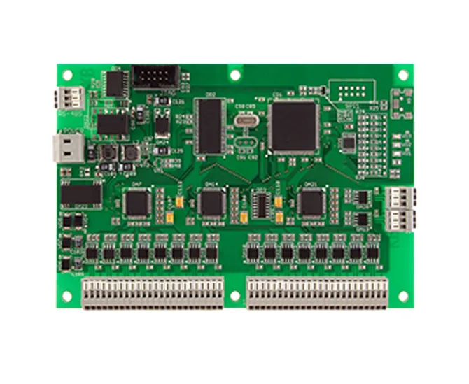
365PCB Printed Circuit Board Assembly Services
365PCB supports PCBA projects from prototype to production, including SMT, THT, and mixed-technology assembly. The service is intended for customers seeking coordinated PCB assembly, component placement, soldering, and testing.
When discussing a project, provide the PCB data, BOM, assembly drawings, production quantity, and testing requirements so the engineering team can evaluate the actual manufacturing scope.
Ultimately, the best PCB Assembly DFM strategy is not to make every board as simple as possible. It is to make each design appropriate for its intended manufacturing process, product requirements, and production volume. That is how design decisions translate into lower avoidable costs and more consistent assembly quality.
Frequently Asked Questions About PCB Assembly DFM
1. What does PCB Assembly DFM mean?
PCB Assembly DFM means Design for Manufacturability applied to printed circuit board assembly. It reviews component selection, footprints, spacing, solder-pad geometry, panelization, inspection access, and manufacturing documentation to make the board easier and more reliable to assemble.
2. What is the difference between PCB DFM and PCB Assembly DFM?
PCB fabrication DFM focuses on manufacturing the bare board, including traces, spacing, drills, vias, stack-up, and materials. PCB Assembly DFM focuses on populating and soldering components, including footprints, placement, soldering, panel handling, inspection, and testing. Both reviews are important for a complete PCBA project.
3. When should PCB Assembly DFM be performed?
Perform PCB Assembly DFM during layout development and before releasing the design for production. A second review is advisable when transferring the design to a new manufacturer, changing components, or moving from prototype to mass production.
4. How does PCB Assembly DFM reduce manufacturing cost?
It can reduce avoidable placement and soldering defects, rework, inspection difficulties, sourcing delays, and engineering clarification cycles. The actual savings depend on design complexity, production volume, manufacturing process, and the issues identified during review.
5. Does PCB Assembly DFM improve product reliability?
It can improve assembly consistency by addressing design-related manufacturing risks. However, DFM alone does not guarantee product reliability. Electrical design validation, component qualification, process control, inspection, and product testing are also necessary.
6. What are the most important PCB Assembly DFM rules?
Prioritize accurate component footprints, suitable pad geometry, adequate component spacing, clear polarity markings, thermal balance, practical panelization, inspection access, and complete manufacturing documentation. The specific design limits should be confirmed with the selected manufacturer.
7. Is SMT better than through-hole assembly for DFM?
SMT is generally suitable for compact layouts and automated production. Through-hole assembly can be appropriate for connectors, mechanically loaded components, and selected power applications. Mixed technology is often the best solution when a product needs both approaches.
8. What standards are relevant to PCB Assembly DFM?
Relevant industry references include IPC standards for PCB design, land patterns, assembly, and acceptability. Examples include IPC-2221 for generic printed board design, IPC-7351 for land pattern design, and IPC-A-610 for acceptability of electronic assemblies. The applicable revision and product class should be agreed by the customer and manufacturer.
9. Can a PCB assembly manufacturer perform DFM for my design?
Many manufacturers provide DFM reviews as part of their engineering or quotation workflow. Ask for a report that identifies manufacturing risks and recommended changes. The design owner should retain approval authority for changes affecting electrical performance, safety, or product requirements.
10. Is PCB Assembly DFM necessary for prototypes?
Yes, although the review can be proportionate to the project's complexity. Basic DFM checks help prevent prototype assembly problems and reveal issues before volume production. For advanced packages or high-density layouts, early DFM review is especially valuable.
References
IPC – Association Connecting Electronics Industries. Industry standards and technical resources for printed circuit board design, electronics assembly, and product acceptability.
IPC Standards. Official information about IPC standards, including design, land pattern, and electronic assembly guidance.
JEDEC – Joint Electron Device Engineering Council. Semiconductor and electronic component standards relevant to package specifications, reliability, and component engineering.