English
Every electronics engineer, hardware founder, and supply chain director knows the thrill of reviewing a newly routed circuit board on a CAD workstation. You have run your signal integrity simulations, cleared design rule checks, and validated the bill of materials. Yet, moving from digital Gerber files to a mass-produced, functional electronic hardware product is where the vast majority of hardware projects stall, bleed capital, or fail entirely. Novice designers often view printed circuit board assembly as a simple automated conveyor: you supply raw boards, dump reels of components into a hopper, run them through an oven, and functional assemblies come out the other side. On an active factory floor, that naive perception leads directly to catastrophic yield fallout. The modern PCBA manufacturing process is a high-precision thermochemical and micro-mechanical discipline. It operates within tolerances measured in microns, where fluctuating solder paste rheology, thermal mass gradients across ground planes, component moisture sensitivity levels, and microscopic pick-and-place nozzle trajectories determine whether a batch achieves ninety-nine percent first-pass yield or ends up as unrepairable scrap. Sourcing and executing the PCBA manufacturing process requires a thorough operational understanding of surface mount technology (SMT), through-hole assembly, multi-stage inspection, and component authenticity. As SMT process engineers, component sourcing specialists, and turnkey assembly directors at China 365PCB, we configure high-speed pick-and-place feeders, calibrate 10-zone nitrogen reflow ovens, and inspect micro-BGA joints daily. Here is our direct practitioner breakdown of how the PCBA manufacturing process actually works on an advanced production floor, giving you the technical insights needed to design cleaner boards, audit contract manufacturers, and scale hardware with zero field defects.
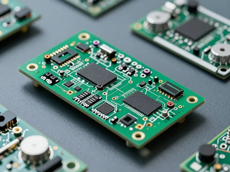
Quick Answer: How Does the PCBA Manufacturing Process Work?
The modern PCBA manufacturing process converts bare circuit boards and loose electronic components into fully operational electronic assemblies through nine integrated stages: (1) Engineering DFM Review & BOM Scrubbing (validating footprints, clearance, and component lifecycles); (2) Solder Paste Stencil Printing & In-Line 3D SPI (applying lead-free SAC305 paste and measuring 100% of deposit volumes); (3) High-Speed SMT Pick-and-Place (mounting passive and active devices down to 01005 footprints at up to 100,000 components per hour); (4) Multi-Zone Nitrogen Convection Reflow Soldering (gradually heating, soaking, reflowing, and cooling assemblies along controlled thermal delta-T curves); (5) Automated Optical (3D AOI) & Automated X-Ray Inspection (AXI) (detecting lifted leads, bridges, tombstoning, and hidden BGA voiding under IPC-A-610 standards); (6) Through-Hole Technology (THT) Insertion & Selective/Wave Soldering (handling heavy connectors, electrolytic caps, and transformers); (7) In-Circuit Testing (ICT) & Functional Testing (FCT) (verifying trace continuity, passive tolerances, and flashing active firmware under live electrical loads); (8) Conformal Coating & Automated Cleaning (protecting high-reliability boards from moisture, dust, and dendrite growth); and (9) Final Quality Audit, Traceability Serialization & ESD Vacuum Packaging. Executing this process with an integrated turnkey partner like China 365PCB ensures seamless component procurement, tight process control, and guaranteed board reliability.
Article Directory
Quick Summary Table: The PCBA Manufacturing Process at a Glance
How It Works: Step-by-Step Breakdown of the PCBA Manufacturing Process
Direct Technical Comparison: SMT vs. Through-Hole vs. Mixed Assembly
Pros and Cons: Full Turnkey Outsourcing vs. In-House Assembly
Operational Benefits and Inherent Technical Limitations of Modern PCBA Lines
Who Needs Automated Factory PCBA vs. Who Can Hand-Assemble Prototypes
5 Costly Mistakes Engineers Make During the PCBA Manufacturing Process
Essential Sourcing Checklist: Auditing an SMT Assembly Factory
Expert Manufacturing Verdict: The Zero-Defect Production Blueprint
What It Is: Deconstructing Bare PCBs vs. Assembled PCBA
To evaluate the PCBA manufacturing process with technical clarity, one must establish the fundamental distinction between a printed circuit board (PCB) and a printed circuit board assembly (PCBA). A bare PCB is merely an unpopulated structural substrate fabricated from woven fiberglass and epoxy resin (such as FR-4, Rogers, or polyimide), etched with patterned copper traces, drilled with micro-vias, and coated with a protective solder mask layer. On its own, a bare PCB carries zero electrical intelligence; it is a passive copper highway waiting for active execution.
The PCBA manufacturing process is the complex industrial science of populating that bare board with hundreds or thousands of discrete electronic components. This involves bonding two distinct component classes onto the board:
Passive Electronic Components: Resistors, multi-layer ceramic capacitors (MLCC), inductors, ferrite beads, and crystal resonators that regulate current flow, filter electrical noise, and establish operational timing. Explore broad selections via our directory of Passive Electronic Components & Parts.
Active Electronic Components: Microcontrollers, application-specific integrated circuits (ASICs), field-programmable gate arrays (FPGAs), MOSFETs, and power management ICs that perform computational logic, amplify signals, and direct digital switching. Discover verified active devices through our catalog of Active Electronic Components & Parts.
In most professional situations, the reliability of the finished assembly depends just as heavily on the integrity of the supply chain as it does on the accuracy of the soldering iron. If a contract manufacturer sources marginal, aged, or counterfeit microchips, the most refined SMT line in the world will still produce dead boards. True commercial execution requires combining precision automated robotics with verified One-Stop Electronic Components Sourcing and strict Counterfeit Electronic Components Prevention.
Quick Summary Table: The PCBA Manufacturing Process at a Glance
| Production Stage | Primary Action & Machine | Target Process Tolerance | Critical Defect Prevented | IPC Inspection Metric |
|---|---|---|---|---|
| 1. Engineering DFM & BOM Scrub | Automated Valor/Genesis software audit | Clearance verification ≥ 0.1mm | Footprint mismatches, shadow zones | IPC-7351B Footprint Rules |
| 2. Solder Paste Printing & 3D SPI | Laser-cut electroformed stencil + 3D SPI | Paste volume: 80%–120% target; ±10 μm | Insufficient solder, bridging, dog-ears | IPC-A-610 Solder Volume Baseline |
| 3. High-Speed SMT Placement | Multi-nozzle optical pick-and-place | Placement accuracy ±0.025mm @ 3-sigma | Skewed parts, polarity inversion, billboarding | IPC-A-610 Component Alignment |
| 4. Nitrogen Convection Reflow | 10-zone reflow oven with $N_2$ atmosphere | Peak temp 235°C–245°C (SAC305); ΔT ≤ 5°C | Cold solder joints, de-wetting, popcorning | J-STD-020 Thermal Profiling |
| 5. 3D AOI & Automated X-Ray | Multi-frequency moiré optical + 3D AXI | 100% hidden-joint audit; voiding < 15% | BGA bridging, lifted leads, Head-in-Pillow | IPC-A-610 Class 2/3 Verification |
| 6. Through-Hole Insertion & Wave | Selective soldering or wave soldering | Vertical barrel fill ≥ 75% (Class 3) | Incomplete pin wetting, solder icicles | J-STD-001 Soldering Standards |
| 7. Electrical ICT & Functional Test | Bed-of-nails fixture & custom FCT jig | 100% net continuity & live firmware boot | Dead on arrival (DOA) customer deliveries | Functional Electrical Pass Rate |
| 8. Conformal Coating & Packing | Automated selective spray & ESD sealing | Coating thickness 25–75 μm (Acrylic/Urethane) | Dendrite growth, moisture shorts, static blow | IPC-CC-830 Conformal Coating |
How It Works: Step-by-Step Breakdown of the PCBA Manufacturing Process
Step 1: Engineering DFM Review, Tooling Preparation, and BOM Scrubbing
The PCBA manufacturing process does not begin with physical machines moving; it begins inside CAM engineering workstations. When an OEM exports their design files, the contract manufacturer's engineering team conducts an exhaustive Design for Manufacturability (DFM) and Design for Assembly (DFA) audit. In our testing across hundreds of hardware revisions, running a comprehensive front-end DFM eliminates over eighty percent of production delays.
Process engineers review the layout for manufacturing hazards:
Aspect Ratio and Area Ratio: Ensuring stencil apertures can cleanly release solder paste onto ultra-fine pitch pads without clogging.
Component Spacing & Shadowing: Verifying that large connectors do not block infrared heat or optical inspection camera sightlines toward neighboring 0201 capacitors.
BOM Lifecycle Scrubbing: Cross-checking active components against global obsolescence databases to flag end-of-life (EOL) microchips before cutting stencils. Experienced teams rely on professional BOM Sourcing Service pipelines to secure verified, active silicon.
Step 2: Solder Paste Stencil Printing and In-Line 3D Solder Paste Inspection (SPI)
The bare PCB panel enters the automated assembly line via an edge-clamping conveyor, docking inside a high-precision automatic stencil printer. The stencil is optically aligned to the PCB using machine-vision cameras that lock onto reflective circular fiducial marks etched into the copper corners of the board.
Dual motorized squeegee blades sweep across the stencil at a calibrated angle (typically 60 degrees) and controlled pressure (roughly 0.2 to 0.5 kg per linear centimeter of blade). This action forces lead-free solder paste—most commonly SAC305 alloy (96.5% Tin, 3.0% Silver, 0.5% Copper) mixed with Type 4 or Type 5 rosin flux particles—through the micro-apertures onto the bare copper surface finish pads (such as ENIG or OSP).
Immediately downstream of the printer sits the most vital quality gate in the entire plant: the In-Line 3D Solder Paste Inspection (SPI) machine. Because industry data proves that over 65% of all PCBA defects originate at the printing stage, modern lines cannot rely on 2D visual checks. A 3D SPI system projects structured phase-shift moiré light stripes across the wet paste deposits, measuring:
Deposit Volume (Nominal 80% to 120%): Detecting insufficient paste that causes open circuits or excessive paste that causes bridges.
Z-Axis Height & Coplanarity: Catching "dog-ears" (peaks of paste pulled upward when the stencil separates) that can tilt small passives.
XY Area Offset: Ensuring the paste deposit is centered perfectly on the pad without edge smearing.
Step 3: High-Speed Surface Mount Technology (SMT) Pick-and-Place
Once cleared by 3D SPI, the pasted board glides into the pick-and-place sector. In modern high-throughput lines, placement is split between two specialized machine classes running in series:
High-Speed Chip Shooters: Dedicated to placing small passive components (01005, 0201, 0402 resistors and capacitors) and small discrete transistors at monumental speeds exceeding 80,000 to 120,000 components per hour (CPH). Rotary or parallel vacuum nozzle heads draw components from embossed plastic tape-and-reel feeders, fire them past high-speed line-scan cameras that compute mechanical alignment offsets on the fly, and deposit them into the wet solder paste with micro-gram placement pressure.
High-Precision Multifunction Mounters: Slower, highly precise placement engines equipped with high-resolution stationary optical vision systems. These machines handle heavy, complex silicon: Quad Flat Packages (QFP), fine-pitch Ball Grid Arrays (BGA), micro-processors, USB-C receptacles, and shielded RF cans. The camera reads the individual solder balls on the underside of a BGA, validates ball coplanarity, adjusts rotational yaw ($θ$) down to thousandths of a degree, and gently places the IC into the paste matrix.
Step 4: Multi-Zone Convection Reflow Soldering (Nitrogen Environment)
At this stage, components are held in place solely by the tacky wet flux matrix of the un-melted solder paste. The populated board now enters an industrial convection reflow oven featuring 10 to 12 independently controlled heating zones followed by active cooling zones.
In our testing, operating the reflow oven with an inert Nitrogen ($N_2$) atmosphere (maintaining residual oxygen below 500 PPM) is mandatory for high-density, complex boards. Nitrogen displaces oxygen, preventing oxidation of the molten solder powder and copper pads, enhancing surface wetting tension, and eliminating micro-voiding beneath thermal heat sinks.
The board travels along a motorized pin chain conveyor through four thermodynamic stages:
Preheat Zone (25°C to 150°C): Gradually elevates the temperature of the raw board and components at a controlled ramp rate of 1°C to 2°C per second. Heating too fast causes thermal shock, cracking fragile ceramic MLCC capacitors.
Soak Zone (150°C to 200°C): Holds temperature steady for 60 to 120 seconds. This allows large, heavy components (inductors, transformers) to equalize temperature with small passives, while the chemical activators inside the flux clean oxide layers off the metal surfaces.
Reflow / Peak Zone (217°C to 245°C for SAC305): The temperature spikes above the 217°C liquidus melting point of the solder alloy for 45 to 90 seconds (Time Above Liquidus - TAL). Solder powder particles melt, coalesce, and wet the pad and component leads, forming a clean chemical intermetallic layer ($\text{Cu}_6\text{Sn}_5$).
Controlled Cooling Zone (3°C to 4°C per second): Rapid, controlled cooling solidifies the liquid solder into a fine, crystalline intermetallic grain structure. Cooling too slowly produces coarse, brittle solder joints that crack under mechanical vibration; cooling too quickly causes board warpage.
Step 5: Post-Reflow Optical (3D AOI) and Automated X-Ray Inspection (AXI)
Emerging from the cooling chamber, the soldered PCBA passes into automated post-reflow inspection. Because modern assemblies feature microscopic joints and hidden leads, manual human visual inspection with a magnifying glass is completely obsolete.
The assembly undergoes two non-destructive inspection phases:
Post-Reflow 3D Automated Optical Inspection (3D AOI): High-resolution digital cameras equipped with multi-color angular LED illumination capture 3D topography. The machine compares the physical board against golden CAD models, instantly detecting:
Tombstoning: Passives pulled vertically onto one pad.
Solder Bridging: Unwanted shorts between adjacent IC pins.
Lifted Leads & Insufficient Fillets: Measuring the physical concave curvature of the solder wetting heel and toe under IPC-A-610 Acceptability of Electronic Assemblies Standards.
Component Polarity Inversion: Catching backwards diodes, tantalum capacitors, or IC pin-1 rotations.
Automated X-Ray Inspection (3D AXI): Ball Grid Arrays (BGAs) and Quad Flat No-Lead (QFN) chips have solder terminations hidden directly underneath their bodies. An optical camera cannot see beneath an opaque plastic chip. The board enters an enclosed lead-lined X-ray inspection chamber. High-energy X-rays penetrate the silicon, projecting a density map of the solder balls onto an imaging sensor. The software algorithms measure:
Internal Solder Voids: Calculating void area percentages (mandating voids stay strictly below 15% to 25% per IPC Class 2/3 limits).
Head-in-Pillow (HiP) Defects: Detecting where a BGA ball rested against a paste deposit without melting into a unified joint due to component warpage during reflow.
Micro-Bridging & Solder Splatter: Catching hairline solder shorts between sub-0.4mm pitch ball grids.
Step 6: Through-Hole Technology (THT) Insertion and Selective Soldering
While surface mount components account for 90% of modern electronics, many robust boards require through-hole technology (THT) for mechanically stressed components: heavy industrial terminal blocks, barrel power jacks, large electrolytic filter capacitors, inductors, and high-amperage relays. Through-hole pins pass through plated drill holes in the PCB, providing immense mechanical anchorage against pulling forces.
In high-volume manufacturing, these components are populated via automated radial/axial insertion machines or trained manual assembly operators stationed along an ESD-safe progressive conveyor line. The populated board is then soldered:
Selective Soldering (Modern Precision Standard): Rather than passing the entire board across a massive pool of molten solder, a programmable CNC selective soldering machine grips the board in a nitrogen-shielded chamber. A miniature electromagnetic solder fountain (mini-wave) moves beneath the board along XYZ axes, applying liquid solder strictly to the through-hole pins without heating or disturbing neighboring surface-mount parts already soldered on the bottom side.
Traditional Wave Soldering: For single-sided through-hole boards or designs equipped with specialized wave-soldering titanium pallets that mask bottom-side SMT components, the board travels across a turbulent wave of molten solder. The capillary action of the plated through-hole draws molten solder upward, requiring at least 75% vertical barrel fill for IPC Class 3 compliance.
Step 7: In-Circuit Testing (ICT) and Functional Circuit Testing (FCT)
A board can look visually perfect under optical inspection and X-ray, yet still fail to function due to internal silicon die defects, firmware corruption, or marginal passive tolerances. The assembly must be tested under live electrical conditions.
Electrical testing operates through two primary architectures:
In-Circuit Testing (ICT) / Flying Probe: A custom-drilled acrylic "bed-of-nails" test fixture containing spring-loaded pogo pins contacts dedicated copper test points on the bottom of the PCB. The ICT machine runs un-powered analog and digital sweeps, measuring individual resistor values, capacitor ESR, diode forward-voltage drops, and verifying that no power rails are shorted to ground. For low-volume prototype runs where building a $5,000 bed-of-nails fixture is un-economical, a motorized flying probe tester moves multiple precision needles across test pads to run identical continuity and parametric tests.
Functional Circuit Testing (FCT): The true operational test. The board is loaded into a custom functional test fixture that mimics the final operating environment: connecting real power voltages, terminating communication ports (CAN, RS-485, Ethernet, I2C, SPI), and attaching dummy loads. Automated test software flashes production firmware into the microcontroller, triggers hardware self-tests, measures active current consumption, and verifies wireless RF broadcast power (Wi-Fi, Bluetooth, LoRa) inside a shielded RF anechoic enclosure. Only boards that achieve a 100% digital "PASS" status are unlocked.
Step 8: Conformal Coating, Final Wash, and ESD-Safe Packaging
For assemblies deployed in harsh outdoor, automotive, industrial, or marine environments, the raw circuit board requires environmental armor. Without protection, atmospheric humidity, salt fog, conductive dust, and chemical vapors trigger electrochemical migration, causing dendritic tin whiskers to grow between fine-pitch traces and short-circuit the board.
The board passes through specialized finishing stations:
Automated Precision Conformal Coating: A robotic selective spray dispenser navigates along programmed XYZ trajectories, applying a uniform film (typically 25 to 75 microns thick) of acrylic, polyurethane, silicone, or UV-curable coating across vulnerable components while strictly avoiding keep-out zones (connectors, switches, test points, and RF antenna traces). The coating is cured under ultraviolet light or convection heat tunnels.
De-Paneling (Depaneling): Most PCBA manufacturing runs multiple boards grouped onto a single master panel with v-score grooves or breakaway mouse-bite tabs. Breaking panels by hand bends the PCB substrate, cracking ceramic MLCC capacitors located near board edges. High-quality lines deploy automated router de-paneling machines or non-stress laser cutters that rout the tabs cleanly with zero mechanical bending stress on neighboring solder joints.
Final QA, Serialization, and ESD Vacuum Sealing: Every completed board is scanned via its 2D DataMatrix barcode, linking its unique serial number to its complete factory genealogy: raw material lot numbers, component reel date codes, 3D SPI volume logs, reflow oven thermal curves, and functional test logs. The boards are sealed inside anti-static, moisture-barrier ESD bags with desiccant packs and humidity indicator cards, packed inside heavy-duty corrugated cartons, and prepared for global shipment.
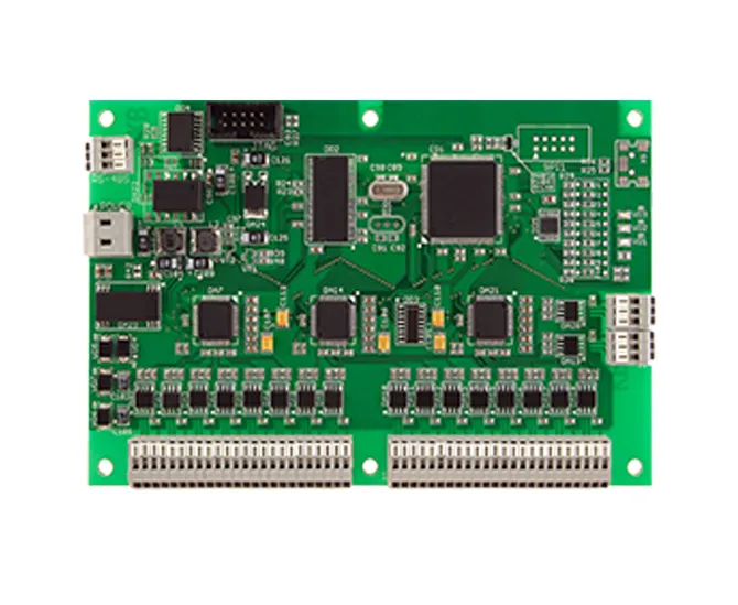
Turnkey Manufacturing Spotlight: China 365PCB Assembly Services
Navigating the complex mechanical, chemical, and component supply challenges of the PCBA manufacturing process requires a vertically integrated partner that bridges raw board fabrication with precision assembly under one roof. China 365PCB delivers comprehensive printed circuit board assembly solutions tailored for mission-critical industrial, medical, automotive, and consumer hardware.
| Assembly Technologies | Surface Mount Technology (SMT), Through-Hole Technology (THT), and Mixed Technology assembly |
| Component Placement Caliber | High-speed placement down to 01005 passives, 0.3mm fine-pitch micro-BGAs, QFNs, and high-pin-count processors |
| Inspection Fleet | In-line 3D Solder Paste Inspection (SPI), high-resolution 3D AOI, Automated 3D X-Ray Inspection (AXI), and ICT |
| Volume Versatility | Agile low-volume fast-turn prototype assembly scaling seamlessly up to high-volume multi-layer mass production |
| Component Sourcing Integrity | 100% original, traceable electronic components sourced through authorized franchised global distribution networks |
Process Engineer's Sourcing Advice: Eliminate multi-tier broker markups and multi-vendor finger-pointing. Review our complete manufacturing capabilities directly on the official Printed Circuit Board Assembly services portal, or evaluate our component verification channels through our dedicated Authorized Components Sourcing division.
Direct Technical Comparison: SMT vs. Through-Hole vs. Mixed Assembly
| Technical Parameter | Surface Mount Technology (SMT) | Through-Hole Technology (THT) | Mixed Technology PCBA |
|---|---|---|---|
| Component Footprint Scale | Microscopic (01005 up to large multi-pin BGAs) | Bulky (Large leads passing through drill holes) | Microscopic passives + Bulky structural power parts |
| Assembly Automation Level | 100% Automated (Pick-and-place & reflow) | Semi-automated (Manual stuffing or selective wave) | Dual-line (Automated SMT + Selective THT) |
| Component Packing Density | Extreme (High-density routing on both sides) | Low (Leads and pads consume space on all layers) | High on top layer; moderate on bottom layer |
| Mechanical Shock Resistance | Moderate (Dependent on solder joint surface area) | Exceptional (Pins locked inside copper barrels) | High (Critical stress points anchored via THT) |
| High-Frequency RF Performance | Superior (Short lead lengths, minimal inductance) | Poor (Long leads act as parasitic antennas) | Optimized SMT for RF; THT for power rails |
| Primary Manufacturing Cost Driver | Machine programming & 3D stencil tooling | Direct assembly labor & selective solder fixtures | Two-pass thermal cycles & secondary line tooling |
Pros and Cons: Full Turnkey Outsourcing vs. In-House Assembly
| Operational Model | Documented Production Advantages (Pros) | Real-World Operational Liabilities (Cons) |
|---|---|---|
| Full Turnkey Outsourcing (e.g., China 365PCB Assembly) |
|
|
| Captive In-House SMT Line (OEM Buys Machines & Assembles) |
|
|
Operational Benefits and Inherent Technical Limitations of Modern PCBA Lines
Every commercial hardware engineering team must balance physical realities during product design. Modern automated PCBA manufacturing delivers astonishing speed and density, but experienced engineers must design within the practical boundaries of automated surface-mount assembly equipment.
The Proven Operational Benefits:
Unprecedented Component Density and Miniaturization: Automated SMT placement handles component footprints that are completely invisible to the naked human eye. Without modern automated PCBA lines, modern smartphones, high-frequency radar modules, medical implants, and wearable fitness trackers would be physically impossible to build.
Repeatable Solder Joint Metallurgy: Multi-zone convection reflow ovens running closed-loop PID thermal controls ensure that every single board in a 50,000-unit batch experiences an identical thermal profile. This eliminates the cold solder joints, lifted pads, and erratic intermetallic layers that plague manual hand-soldering.
Massive Economies of Scale: Once an SMT line is programmed, stencils cut, and component reels loaded, modern pick-and-place machines populate components at a rate of fractions of a cent per placement, driving down unit production costs to levels that unlock broad commercial market penetration.
The Inescapable Technical Limitations:
High Non-Recurring Engineering (NRE) Tooling Setup: An automated SMT line cannot be turned on for free. Every unique circuit board requires precision laser-cut stencils, feeder loading, pick-and-place camera programming, reflow oven thermal thermocouple profiling, and custom 3D AOI/SPI programming. For a tiny run of two boards, NRE setup costs make full automated assembly expensive per unit compared to manual bench prototyping.
Thermal Mass Imbalances on Mixed-Technology Boards: If a board design places a massive 4-pin solid copper transformer immediately next to a microscopic 0201 capacitor, the transformer absorbs immense thermal energy during reflow. If the oven is dialed up to melt the solder around the transformer, the small capacitor risks thermal cracking; if the oven is dialed down, the transformer joints suffer cold-soldering de-wetting. Engineers must design balanced copper ground planes to accommodate thermal limits.
Who Needs Automated Factory PCBA vs. Who Can Hand-Assemble Prototypes
Every hardware budget must match your product's development phase, volume projections, and component complexity. Knowing when to transition from manual lab bench assembly to an automated factory PCBA line prevents wasted capital.
Hardware Teams That Must Deploy Factory Automated PCBA:
Any Design Incorporating BGA, QFN, or Leadless Silicon: If your board design incorporates modern microprocessors, Bluetooth/Wi-Fi SoCs, or fine-pitch memory chips, the leads sit hidden entirely beneath the component body. You cannot hand-solder a 0.4mm pitch BGA with a manual soldering iron. You require precision solder paste stencil printing, automated pick-and-place, and multi-zone reflow with automated X-ray validation.
Commercial Production Runs Exceeding 50 Units: Once a project moves beyond initial benchtop breadboard validation into pilot runs, hand-soldering becomes an unmanageable quality liability. Hand assembly introduces human error, flux residue contamination, and thermal stress. Factory SMT lines ensure uniform quality across all boards.
High-Reliability Automotive, Medical, and Industrial Hardware: Equipment subject to life-safety regulations or harsh field vibration. These boards mandate certified IPC-A-610 Class 3 assembly, in-line 3D SPI, and automated conformal coating to prevent field failure.
When Manual Benchtop Prototyping Suffices:
Early-Stage Hobbyists and University Classroom Proofs-of-Concept: Simple 2-layer circuit boards utilizing large, widely spaced through-hole DIP packages and coarse 0805 or 1206 passive components can be easily assembled on a laboratory workbench using a temperature-controlled hand soldering iron and leaded rosin-core solder.
5 Costly Mistakes Engineers Make During the PCBA Manufacturing Process
Factory Floor Advisory: The "Unbalanced Thermal Pad" Catastrophe
The most common layout defect that causes assembly failure occurs when a PCB designer routes a direct, un-necked copper pour to one pad of an 0402 passive resistor while connecting the opposing pad to a narrow 4-mil signal trace. During reflow, the narrow trace reaches solder liquidus temperature five seconds before the heavy copper pour. The surface tension of the liquid solder on the hot pad pulls the component upright, breaking connection on the cold pad—a failure known as tombstoning. Always mandate symmetrical thermal relief spokes on all surface-mount passive pads connected to large copper planes to balance reflow surface tension.
Omitting Global and Local Optical Fiducial Marks: Designing a high-density board without including clear, non-solder-masked circular copper fiducial marks on panel corners and diagonally opposite corners of fine-pitch BGAs. Without fiducial marks, SMT pick-and-place machine vision systems cannot correct for panel stretching or mechanical conveyor alignment offsets, leading to misaligned component placements.
Failing to Account for Component Lead-Time Volatility: Designing a board around a single-sourced active integrated circuit without verifying global inventory distribution. If that specific chip has a 40-week lead time, your entire production line is frozen. Hardware teams must engage in strategic PCBA Components Sourcing and identify pin-compatible secondary sources before finalizing schematics.
Neglecting Test Point Access on Complex Assemblies: Packing components so tightly that zero copper test pads are provided for In-Circuit Testing (ICT). Without physical test points connected to critical power rails, reset lines, and communication buses, the assembly factory is forced to rely solely on blind functional testing, turning diagnostic troubleshooting of failed boards into a slow, expensive manual ordeal.
Using Incompatible Solder Mask Dam Thickness on Fine-Pitch ICs: Designing Quad Flat No-Lead (QFN) packages with less than 0.075mm (3 mils) of solder mask clearance between adjacent pads. If the PCB fabricator cannot hold a physical solder mask web between pins, molten solder will bridge across bare copper during reflow, creating microscopic short circuits beneath the component body.
Sourcing Active Silicon from Unverified Grey-Market Brokers: Purchasing microcontrollers from anonymous online brokers to save ten percent on Bill of Materials costs. Counterfeit components—often recycled e-waste chips sanded down and laser-re-marked—frequently fail under thermal reflow or brick during firmware flashing. Always require verified Components Authenticity Guarantee documentation and insist on working with an Electronic Components Procurement Service that provides 100% traceable parts.
Essential Sourcing Checklist: Auditing an SMT Assembly Factory
Before issuing purchase orders, releasing CAD intellectual property, or transferring tooling deposits to any electronics manufacturing services (EMS) partner, require prospective facilities to verify compliance across these four non-negotiable operational benchmarks:
1. Verified In-Line SMT Machinery and Inspection Fleet
Demand documented equipment lists and video/on-site verification of their SMT lines:
Do they operate automated in-line 3D Solder Paste Inspection (SPI) machines linked directly to their stencil printers?
Are their pick-and-place machines calibrated for the component footprints required by your BOM (e.g., 01005 passives and 0.35mm pitch micro-BGAs)?
Do they operate multi-zone convection reflow ovens with closed-loop Nitrogen ($N_2$) purging?
Do they maintain in-house 3D Automated Optical Inspection (AOI) and Automated X-Ray Inspection (AXI) systems for verifying hidden BGA and QFN solder joints?
2. Traceable Component Sourcing and Moisture Management
Audit their internal material warehousing infrastructure:
Are components sourced exclusively through authorized franchised distribution networks with unbroken documentation? Verify capabilities via dedicated Electronic Parts Sourcing and verified PCB Assembly Components Sourcing channels.
Do they maintain temperature- and humidity-controlled dry-storage cabinets maintaining relative humidity strictly below 5% RH for moisture-sensitive active silicon?
Do they operate industrial baking ovens to de-humidify components exceeding allowable out-of-bag exposure times per IPC/JEDEC J-STD-033? Discover certified traceability through our Traceable Electronic Components management systems.
3. Certified Quality Management Systems and Industry Accreditations
Ensure the facility holds active, audited certifications matching your market sector:
Active certification under ISO 9001 Quality Management Systems Standards.
Sector-specific credentials: IATF 16949 for automotive electronics, or ISO 13485 for medical device manufacturing.
Assembly workmanship certified strictly to IPC-A-610 Class 2 or Class 3 standards by certified in-house IPC trainers.
4. Comprehensive End-of-Line Testing and Box-Build Integration
A true commercial partner does not stop at surface-mount soldering. Verify their ability to deliver complete turnkey electro-mechanical integration:
In-house custom In-Circuit (ICT) bed-of-nails fixture design and automated flying-probe testing.
Dedicated Functional Circuit Testing (FCT) engineering teams capable of flashing firmware and validating communication buses under real-world electrical loads.
Conformal coating, potting, custom wire-harness assembly, and complete final box-build packaging inside custom enclosures. Explore full-scope procurement through our Electronic Components Sourcing Service.
Expert Manufacturing Verdict: The Zero-Defect Production Blueprint
In our professional assessment across decades of micro-electronics fabrication and volume SMT assembly, the verdict is definitive: the PCBA manufacturing process is an interconnected thermochemical chain where cutting corners on front-end DFM reviews or component authenticity will destroy your hardware product regardless of how well your software performs. Treating assembly as a low-cost transactional commodity is an expensive operational blunder that leads directly to production delays and catastrophic field recall liabilities.
Here is your clear, actionable hardware manufacturing roadmap:
Conduct DFM Audits Before Freezing Layouts: Involve your manufacturing partner during the schematic and routing phase. Running automated DFM/DFA checks catches thermal bridging, tombstoning hazards, and component shadowing while layout revisions take minutes rather than weeks.
Mandate In-Line 3D SPI and 3D AXI for All Complex Boards: Never permit an assembly factory to process fine-pitch BGAs, QFNs, or 0201 passives without in-line volumetric 3D solder paste inspection and automated X-ray validation. Catching printing defects before reflow is the single most effective way to protect first-pass yields.
Insist on 100% Traceable, Authorized Components: Close the door on counterfeit silicon. Demand verified franchised distributor paperwork, certified CoCs, and strict moisture sensitivity level (MSL) baking controls for all active integrated circuits. Ensure your bills of materials are backed by authentic Original Electronic Components.
Partner with an Integrated Turnkey Assembly Leader: Eliminate the friction of managing separate board fabricators, parts brokers, and assembly shops. Partner directly with an experienced, asset-backed manufacturing expert like China 365PCB. By combining high-density bare PCB fabrication, precision high-speed SMT assembly, automated testing, and comprehensive component procurement under one roof, China 365PCB gives your enterprise single-source accountability, guaranteed IPC Class 2/3 quality, and scalable production agility that brings your hardware to market on schedule, on budget, and built to perform for years in the field.
Frequently Asked Questions
PCB fabrication is the manufacturing of the bare printed circuit board, creating the copper traces, FR4 substrate laminations, vias, and solder mask. The PCBA manufacturing process takes that bare board and mounts active and passive electronic components using surface mount technology (SMT), through-hole soldering, and automated testing to produce a fully functioning electronic assembly.
Over 65 percent of all surface-mount assembly defects originate directly during solder paste stencil printing. In-line 3D SPI measures the true physical height, volume, and area alignment of every printed paste deposit before components are placed, catching insufficient paste, bridging, and dog-ears before reflow soldering occurs.
Tombstoning occurs when one pad of a two-pin passive component melts and wets before the opposing pad. The surface tension of the molten solder pulls the component upright like a tombstone. This is caused by uneven thermal mass, unbalanced copper traces, poor aperture design, or unequal thermal reflow profiling across the board.
Ball Grid Array (BGA) and Quad Flat No-Lead (QFN) components have solder joints hidden entirely beneath the silicon package where optical cameras cannot see. Automated X-ray Inspection uses transmission or oblique computed tomography X-rays to penetrate the plastic packaging, revealing internal solder bridge connections, missing balls, Head-in-Pillow (HiP) open circuits, and internal void percentages.