In the world of electronics manufacturing, hardware engineers frequently take the foundational substrate of their designs for granted. Before the 1950s, electronic devices relied on point-to-point wire wrapping—a chaotic, error-prone, and unscalable method of connecting components. Today, understanding the true purposes of a printed circuit board (PCB) is the difference between a prototype that works on a test bench and a commercially viable product that survives global distribution.
From our experience at China 365PCB, managing over 100,000 square meters of self-owned production area, we see companies miscalculate their substrate needs daily. They treat the PCB as a simple piece of fiberglass when, in reality, it is the most critical mechanical and electrical component in their entire bill of materials. In this guide, we break down the engineering realities, exposing exactly why you use a PCB, when to upgrade your materials, and how professional manufacturers approach bare board fabrication.
Quick Answer: What are the Purposes of a Printed Circuit Board?
The primary purposes of a printed circuit board are to provide mechanical support for electronic components and to facilitate reliable electrical interconnection through conductive copper pathways. Beyond simple wiring, a PCB manages thermal dissipation, shields against electromagnetic interference (EMI), controls high-speed signal impedance, and allows for automated mass production via Surface Mount Technology (SMT).
Whether you are designing a consumer IoT device or an aerospace navigation system, the PCB is the physical foundation that makes electronic miniaturization, scalability, and ruggedness possible.
What is a PCB and How Does it Work?
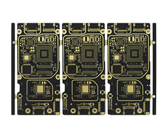
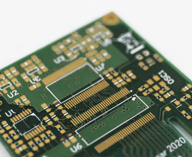
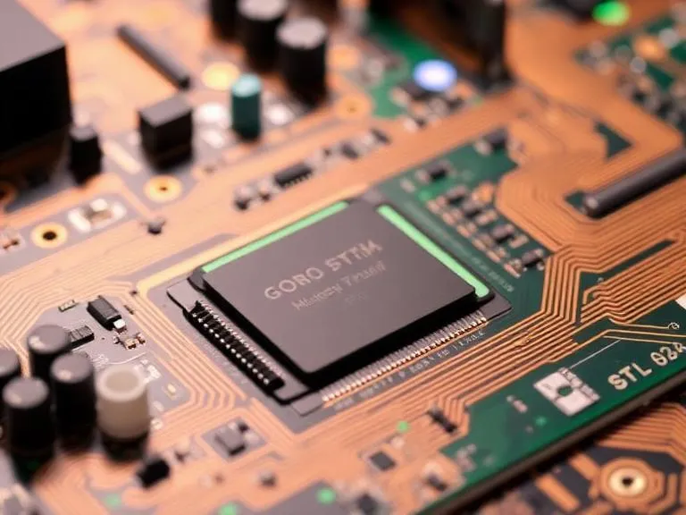
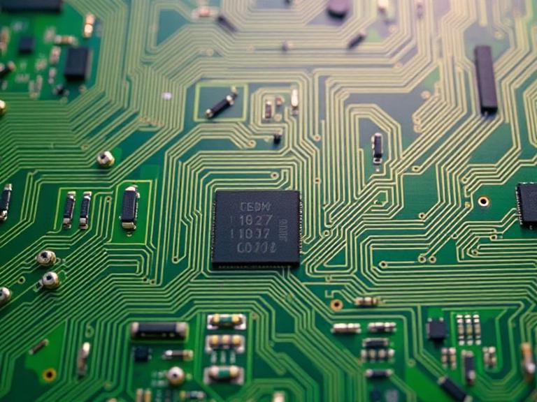
At its core, a printed circuit board is a composite structure consisting of an insulating dielectric material—typically FR4 fiberglass—laminated with one or more layers of conductive copper. The copper is chemically etched away using photolithography to leave behind specific traces, pads, and vias. These remaining copper features act as the "wires" that connect your microcontrollers, resistors, and integrated circuits.
How it works is a matter of precision manufacturing. A component is placed onto the copper pads, and solder (a metal alloy) is melted to create both an electrical and mechanical bond. In a Multilayer PCB, internal copper layers are connected to external layers using plated through-holes (vias). This allows engineers to route complex schematics without copper lines crossing and short-circuiting each other. In most professional situations, the board is then coated in a solder mask (the green, blue, or black layer) to prevent solder bridges and protect the copper from oxidation.
The 20 Core Purposes of a Printed Circuit Board
To truly understand the engineering value of your substrate, you must look beyond basic connectivity. Here are the 20 distinct purposes of a printed circuit board in modern manufacturing.
Mechanical Component Support: The rigidity of the fiberglass substrate holds heavy components like transformers and relays securely in place, preventing vibration-induced failure.
Electrical Routing: Copper traces replace bulky wires, allowing for precise, predictable, and microscopic electrical connections between components.
Form Factor Miniaturization: By utilizing Blind Via PCB technology, engineers can stack components and routing paths, shrinking a device from the size of a shoebox to the size of a smartwatch.
Automated Assembly (SMT): PCBs are designed to be run through automated Pick-and-Place machines and reflow ovens, a purpose that makes mass production economically viable.
Thermal Management: Heavy copper planes and thermal vias draw heat away from high-power components (like CPUs and MOSFETs), preventing thermal runaway.
Impedance Control: For high-speed data (like USB-C or HDMI), the width and spacing of PCB traces are calculated to maintain a specific impedance, preventing signal reflection and data loss.
Electromagnetic Interference (EMI) Shielding: Internal ground planes in a multilayer board act as Faraday cages, absorbing stray RF noise and preventing the device from failing EMC compliance testing.
Power Distribution: Dedicated power planes allow clean, low-inductance voltage to reach hundreds of pins simultaneously without voltage drops.
Fault Diagnostics: Silkscreen labels (reference designators) are printed directly onto the board, allowing technicians to locate test points and troubleshoot failed components rapidly.
High-Frequency Transmission: Utilizing specialized materials like a PTFE PCB allows microwave and radar signals to travel with minimal dielectric loss.
Environmental Protection: The board serves as a stable base for conformal coating and potting, sealing the circuit away from moisture, dust, and corrosive chemicals.
Standardized Integration: Edge connectors and gold fingers on the PCB allow the board to be slotted into standardized racks, such as PCIe slots in computer motherboards.
High-Voltage Isolation: By engineering precise creepage and clearance distances into the board layout, PCBs prevent high-voltage arcing between traces.
Cost Reduction: Once the initial tooling is paid for, manufacturing a PCB is exponentially cheaper and faster than paying humans to manually solder wires.
Consistent Performance: Because every board is etched from a photographic master file, board #1 performs exactly the same as board #100,000, ensuring absolute product consistency.
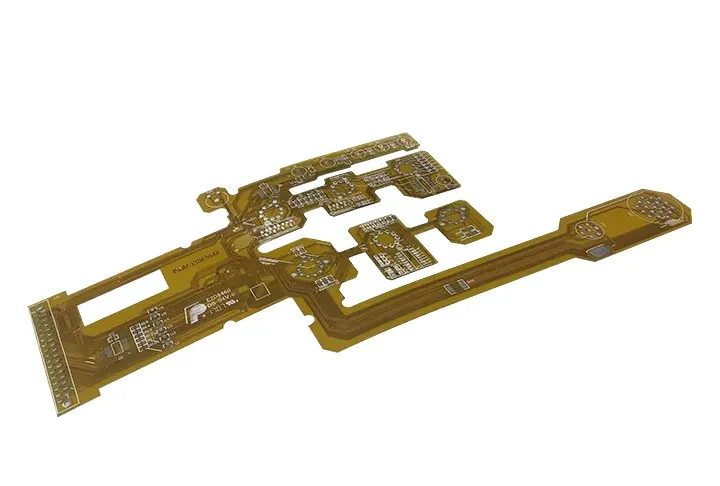
3D Packaging: Rigid-flex and multilayer boards allow electronics to be folded and contoured to fit into non-linear housings, such as camera lenses or aerospace fuselages.
Extreme Temperature Survival: For automotive and aerospace engines, a Ceramic PCB serves the purpose of operating flawlessly in environments exceeding 300°C where standard fiberglass would instantly burn.
Component Footprint Standardization: PCBs force the industry to adopt standardized component packages (like 0402 or 0805 resistors), streamlining global supply chains.
Weight Reduction: Compared to heavy wiring harnesses and terminal blocks, a PCB drastically reduces the payload weight in drones, satellites, and electric vehicles.
IP Protection: Burying proprietary routing logic inside the internal layers of a 12-layer board makes it exceptionally difficult for competitors to reverse-engineer your product.
Benefits and Limitations (Pros vs Cons)
In our testing and manufacturing history, we always advise clients to weigh the realities of bare board fabrication. While PCBs are the undisputed king of electronics manufacturing, they have specific limitations.
Pros and Cons Table: PCB Implementation| Benefits of PCBs | Limitations of PCBs |
|---|
| Unmatched scalability for mass production via automated SMT lines. | High upfront tooling and NRE (Non-Recurring Engineering) costs for prototypes. |
| Eliminates human error associated with manual wire routing. | Difficult to modify once fabricated; errors usually require a complete board respin. |
| Exceptional high-speed signal integrity and impedance control. | Standard FR4 cannot handle extreme heat; requires expensive ceramic or metal-core upgrades. |
| Compact size reduces shipping costs and enclosure tooling costs. | Environmental impact; the etching process utilizes heavy chemicals requiring strict disposal. |
Comparison Table: Choosing the Right PCB Type
Not all purposes of a printed circuit board are served by the same material. We recommend matching your application strictly to the substrate class to avoid commercial failure.
Quick Summary Table: PCB Variants| PCB Type | Primary Purpose & Use Case | Relative Cost |
|---|
| Single Sided PCB | Basic consumer goods, power supplies, LED lighting (low density). | Very Low |
| Multilayer PCB (4-32 Layers) | Smartphones, medical devices, computers, high-speed data routing. | Medium to High |
| Ceramic PCB | Automotive sensors, aerospace, high-power LED arrays (extreme thermal). | High |
| FR2 PCB | Ultra-cheap consumer electronics (paper/phenolic base, no through-holes). | Lowest |
| PTFE PCB | Radar, 5G base stations, microwave RF equipment (low signal loss). | Very High |
Who Should Use It & Who Does Not Need It
For commercial users and hardware startups: You absolutely must design your product around a PCB. Bringing a device to market using breadboards or point-to-point wiring is commercial suicide. Regulatory bodies (FCC, CE, UL) will instantly fail devices that do not use properly engineered PCBs to control emissions and electrical safety.
For heavy-duty applications: Industrial automation and military contractors should utilize heavy-copper PCBs or a Through-Hole PCB for components that endure massive physical shock and vibration. SMT components can shear off under extreme G-forces, whereas through-hole leads anchor the component physically to the board.
Who does not need it: Hobbyists experimenting with initial circuit logic do not need to order a custom PCB. Stick to solderless breadboards until your schematic is 100% validated. Furthermore, high-amperage industrial power grid applications (handling hundreds of amps) generally rely on copper busbars rather than printed circuit boards, as even thick copper PCBs will delaminate under massive current loads.
Common Mistakes in PCB Sourcing
The most devastating mistake we see engineers make is failing to specify the glass transition temperature (Tg) of their FR4 material. If you are building a device that operates in a hot environment (like under a car hood) and you source cheap standard Tg130 FR4, the board will expand, the vias will crack, and the device will die within a month. Always specify High-Tg (Tg170+) for demanding environments.
Another common error is ignoring design for manufacturability (DFM). Designers often place components too close to the board edge or fail to add fiducial marks. When the files arrive at a facility like China 365PCB, our automated SMT machines cannot properly grip or align the board, resulting in frustrating production delays and costly redesigns.
Buying Considerations
When you are ready to move from design to procurement, use commercial judgment. Do not simply buy from the cheapest broker online. Use this buying guide table to vet your manufacturer.
Buying Guide Table: Vetting a PCB Manufacturer| Specification / Capability | What to Look For | Why It Matters |
|---|
| Facility Ownership | Direct manufacturer (not a broker). | Brokers add markup and lose control over quality. Direct fabs ensure traceability. |
| Testing Standards | 100% AOI, E-Test, and Flying Probe. | Without electrical testing, you will pay for short-circuited boards that destroy your expensive ICs. |
| Material Certifications | UL listing, RoHS compliance, ISO9001. | Customs will seize products that cannot prove RoHS compliance for hazardous substances. |
| Turnkey Capability | Fab, Sourcing, and SMT Assembly in-house. | Shipping bare boards to a separate assembly house increases freight costs, lead times, and finger-pointing if something fails. |
Expert Recommendation
The China 365PCB Verdict
From our experience managing end-to-end OEM/ODM solutions, the purposes of a printed circuit board extend far beyond the schematic. The PCB is the mechanical chassis and thermal heatsink of your product. We strongly recommend that commercial buyers stop treating PCB fabrication as a commodity purchase.
At China 365PCB, our 100,000 square meter self-owned facility ensures that whether you need a basic single-sided board for a toy or a complex 20-layer blind/buried via board for telecommunications, you receive absolute quality control. For modern electronics, we advise skipping cheap FR2 entirely. Invest in high-quality FR4 or advanced laminates, partner with a full-industry-chain manufacturer to handle both fabrication and SMT, and secure your supply chain against global disruptions.
Frequently Asked Questions
What is the main purpose of a printed circuit board?
The main purpose of a printed circuit board is to mechanically support electronic components and electrically connect them using conductive copper tracks etched from copper sheets laminated onto a non-conductive substrate. This eliminates bulky wires and allows for automated mass production.
Why do PCBs use copper instead of other metals?
Copper is used because it offers an exceptional balance of high electrical conductivity, excellent heat dissipation, and cost-effectiveness. While silver is slightly more conductive, it is too expensive for mass production. Copper can also be easily etched using standard chemical processes.
Can a PCB operate in extreme high temperatures?
Standard FR4 PCBs begin to degrade above 130°C to 170°C. If your application requires extreme heat survival (such as inside an engine block or aerospace exhaust), you must use specialized substrates like Ceramic PCBs or Polyimide, which can withstand temperatures exceeding 250°C without delaminating.
References & Industry Standards
 English