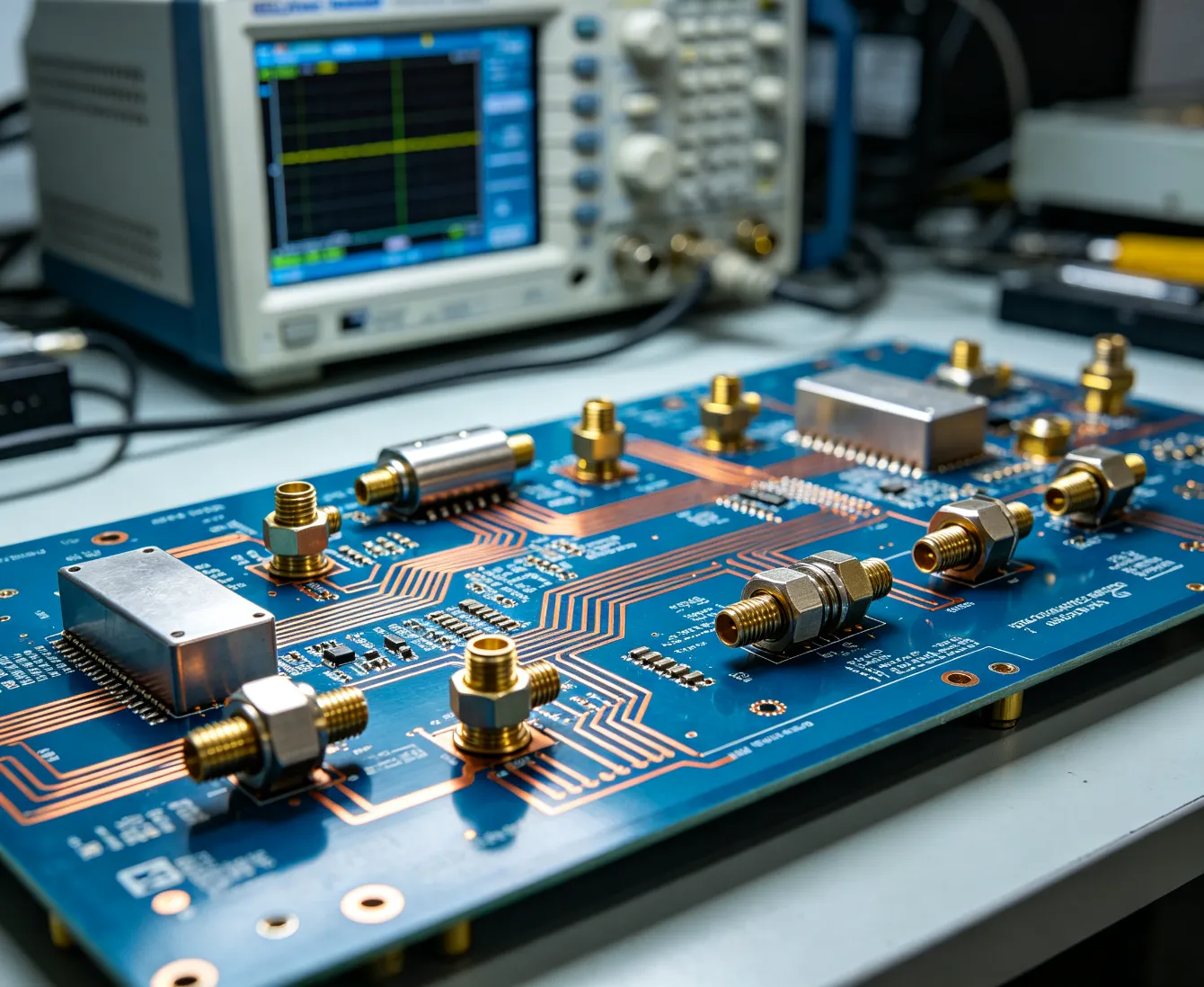
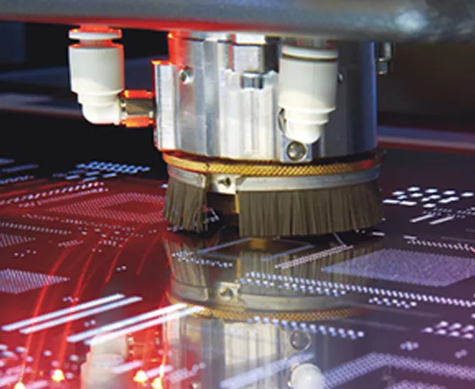
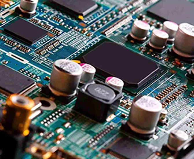
The electronic hardware landscape is undergoing a brutal transition. Products are shrinking, operational frequencies are skyrocketing into the gigahertz range, and power density requirements are melting conventional substrates. If your engineering team is still relying solely on standard two-layer or four-layer fiberglass boards, your product roadmap is likely already obsolete. To survive in telecommunications, aerospace, medical devices, and high-performance computing, you must understand and implement advanced PCBs.
From our experience as a primary manufacturer at China 365PCB, the disconnect between hardware designers and fabrication realities is the number one cause of project failure. Designers often over-engineer boards, driving unit economics into the ground, or under-engineer them, leading to catastrophic thermal failures in the field. In this comprehensive guide, we will strip away the marketing jargon and deliver an unvarnished look at what advanced PCBs actually are. We will explain how these technologies work, whether your specific project requires them, and how to apply commercial and practical judgment when sourcing them.
Quick Answer: Defining Advanced PCBs
Advanced PCBs are highly engineered printed circuit boards that transcend the capabilities of standard mechanical drilling and basic FR4 materials. They utilize sophisticated manufacturing techniques such as sequential lamination, laser-drilled microvias, and exotic substrates (like PTFE, ceramic, or polyimide). This category includes High-Density Interconnect (HDI) boards, rigid-flex circuits, high-frequency RF boards, and heavy copper power boards. Advanced PCBs are required when standard boards cannot meet the necessary demands for extreme miniaturization, high-speed signal integrity, dynamic mechanical flexing, or massive thermal dissipation.
What It Is: The Anatomy of Advanced PCBs
To establish a baseline, a standard FR4 PCB uses woven fiberglass cloth with an epoxy resin binder, relies on through-hole mechanical drilling, and features straightforward copper tracing. It is robust, cheap, and perfect for simple logic circuits and basic consumer electronics.
Advanced PCBs throw these limitations out the window. They are categorized not by a single feature, but by a combination of high-end capabilities:
High-Density Interconnect (HDI): When you run out of real estate on a board, you must go dense. An HDI PCB packs more functionality into a smaller area by utilizing blind vias, buried vias, and microvias. This allows for complex routing out of fine-pitch components like Ball Grid Arrays (BGAs).
Exotic Substrates: Advanced boards for radar, 5G, or satellite communications abandon standard FR4. Instead, a High-Frequency PCB uses materials like Rogers, Taconic, or PTFE. These materials possess tightly controlled dielectric constants (Dk) and incredibly low dissipation factors (Df), ensuring high-speed signals do not degrade or reflect.
Mechanical Flexibility: For wearables, medical implants, or aerospace folding mechanisms, rigid boards fail. A Rigid Flex PCB combines flexible polyimide ribbons integrated directly into rigid FR4 sections, eliminating the need for bulky connectors and wiring harnesses.
Thermal and Power Management: For heavy-duty applications like electric vehicle (EV) charging stations or high-power LED arrays, standard copper traces will melt. A Heavy Copper PCB (using 3 oz to 20 oz copper) carries massive current, while a Metal Core PCB acts as an active heat sink to dissipate thermal loads rapidly.
How It Works: Fabrication Realities
The magic of advanced PCBs lies not just in the design file, but in the brutal realities of the manufacturing floor. In most professional situations, engineers overlook the physical processes required to build their designs.
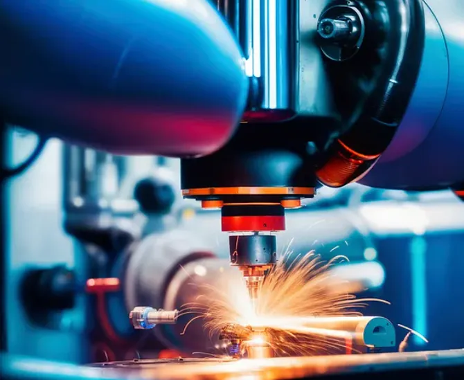
Consider microvias. Standard drill bits snap if they are smaller than 0.15mm (6 mils). To achieve the density required for an HDI board, we must deploy a Laser Drilled PCB process. High-energy UV or CO2 lasers vaporize the epoxy and glass down to the target copper pad without penetrating it.
Furthermore, advanced boards require sequential lamination. A standard board is pressed together in a single high-heat, high-pressure cycle. An advanced 10-layer HDI board with blind and buried vias might require three or four separate pressing and drilling cycles. Each sequential lamination cycle exponentially increases manufacturing time, cost, and the risk of layer misregistration.
Quick Summary Table: Advanced PCB Technologies| Technology Type | Defining Characteristic | Primary Application |
|---|
| HDI (High-Density Interconnect) | Microvias, sequential lamination, fine lines. | Smartphones, IoT devices, dense BGA routing. |
| Rigid-Flex | Polyimide flexible layers combined with rigid FR4. | Aerospace, medical devices, folding mechanisms. |
| High-Frequency / RF | PTFE/Teflon substrates, strict impedance control. | 5G telecom, radar, satellite transceivers. |
| Metal Core / Heavy Copper | Aluminum/copper backing, >3oz copper traces. | High-power LEDs, EV power inverters. |
The Unmatched Benefits
In our testing, the transition from conventional to advanced PCBs yields definitive commercial advantages that justify the higher capital expenditure.
First, miniaturization. You cannot build a modern smartwatch or a discrete medical diagnostic tool using mechanical through-hole vias. HDI technology allows you to shrink a 10-inch board down to a 2-inch footprint while retaining all functionality.
Second, signal integrity. As processing speeds increase, a standard Double Sided PCB becomes an antenna, radiating noise and failing EMI/EMC compliance tests. Advanced routing on specialized substrates guarantees that your 10 Gbps data lines reach their destination without jitter, crosstalk, or attenuation.
Third, reliability in harsh environments. Utilizing a premium surface finish like an ENIG(Electroless Nickel Immersion Gold)PCB prevents oxidation and ensures flawless solder joints, which is mandatory for aerospace and defense hardware that cannot fail in the field.
Limitations and Manufacturing Bottlenecks
We recommend approaching advanced PCBs with your eyes wide open. The limitations are stark and primarily financial. Because these boards require exotic materials, laser drilling, and multiple pressing cycles, the unit cost can be 300% to 1000% higher than a standard board.
Moreover, yield rates drop as complexity increases. If a standard board has a manufacturing yield of 98%, an aggressive 12-layer Any-Layer HDI board might have a yield of 85%. You are paying for the scrapped boards. Lead times also increase dramatically. You can get a standard board fabricated in 24 hours; a complex rigid-flex board will take weeks.
Comparison Table: Standard vs. Advanced PCBs| Specification | Standard PCB (FR4) | Advanced PCB |
|---|
| Via Technology | Mechanical Through-Hole | Laser Microvias, Blind/Buried, Via-in-Pad |
| Material | Standard Epoxy Glass (FR4) | PTFE, Polyimide, Ceramic, Aluminum |
| Trace Width / Spacing | > 4 mils (0.1mm) | < 3 mils, down to 1.5 mils |
| Cost Profile | Low, highly commoditized | High, requires specialized fabrication |
| Lead Time | 1 - 3 Days | 2 - 4 Weeks |
Who Should Use It & Who Does Not Need It
For commercial users and innovators: If you are designing 5G infrastructure, autonomous vehicle LiDAR systems, implantable medical devices, or high-end consumer electronics, you must use advanced PCBs. There is no alternative. The physics of your application demand controlled impedance, dense packaging, or extreme thermal dissipation.
Who does not need it: For beginners, hobbyists, or engineers designing simple logic controllers, power supplies, or basic white-goods appliances. If your circuit can fit on a standard 4-layer FR4 board using a Single Sided PCB or double-sided routing, do not use HDI. Over-engineering a simple product with blind vias and exotic Teflon materials destroys your profit margin for absolutely zero functional gain.
Pros and Cons of Implementing Advanced PCBs| Pros (Benefits) | Cons (Limitations) |
|---|
| Enables extreme miniaturization and dense component packaging. | Significantly higher unit cost and NRE (Non-Recurring Engineering) fees. |
| Flawless signal integrity for high-speed digital and RF applications. | Longer manufacturing lead times due to sequential lamination. |
| Eliminates bulky wire harnesses (via Rigid-Flex tech). | Lower manufacturing yield rates compared to standard boards. |
| Superior thermal management for high-power components. | Requires fabricators with specialized, expensive equipment (lasers, plasma). |
Common Mistakes in Design and Procurement
From our experience auditing client Gerber files, the most catastrophic mistake is designing an advanced PCB without consulting the fabricator's capabilities. Designers will specify an asymmetric stack-up that inevitably warps and bows inside the reflow oven, rendering the board useless.
Another prevalent error is calling out highly specific, exotic raw materials (like a specific Rogers substrate) that have a 16-week lead time from the laminate supplier. In most professional situations, you should specify the required electrical properties (Dk, Df, Tg) and allow your fabrication partner to select an equivalent material they already have in stock.
Buying Considerations for Commercial Users
When you are ready to transition your product line to advanced PCBs, your procurement strategy must shift. You can no longer rely on anonymous online broker platforms that outsource your design to the lowest bidder. Advanced boards require tight engineering feedback loops (Design for Manufacturing - DFM).
You must evaluate your fabrication partner based on their internal equipment. Do they own their own laser drills? Do they have plasma desmear machines for rigid-flex? Do they offer a dedicated PCB Prototype Service that uses the exact same production line as their volume manufacturing? If a vendor outsources their laser drilling, you will suffer from quality control failures and delays.
Buying Guide: Evaluating an Advanced PCB Fabricator| Evaluation Criteria | What to Look For | Why It Matters |
|---|
| Facility Ownership | Self-owned and self-managed facilities. | Brokers cannot guarantee traceability or control sequential lamination quality. |
| DFM Support | Pre-production engineering review. | Catches impedance mismatches and via-aspect-ratio failures before fabrication. |
| Material Inventory | Stocked high-frequency and polyimide laminates. | Prevents 10+ week delays waiting for exotic substrates to arrive. |
| Testing Capabilities | In-house TDR (Time Domain Reflectometry), Flying Probe. | Guarantees signal integrity and identifies microvia failures before shipping. |
Expert Recommendation from China 365PCB
In most professional situations, the success of your advanced PCB project hinges entirely on the transparency and capability of your manufacturing partner. Designing a dense HDI board or a complex rigid-flex circuit is only half the battle; executing it with high yield rates and cost-efficiency requires a world-class facility.
China 365PCB is a self-operated electronics manufacturing group integrating PCB fabrication, SMT assembly, electronic component sourcing, CNC and 3D printing, cable harness assembly, and OEM/ODM production support.
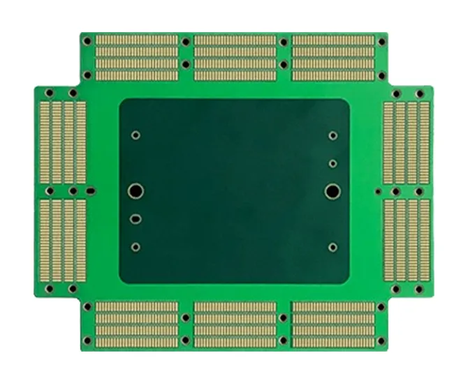
We strongly recommend abandoning fragmented supply chains. When you separate your advanced PCB fabrication from your SMT assembly, you invite finger-pointing when a BGA component fails to solder correctly onto a microvia-in-pad. With more than 15 years of manufacturing experience and over 100,000㎡ of production area, our facilities are self-owned and self-managed. This structure supports faster internal coordination, consistent process control, production traceability and flexible project scheduling. Whether you need a bleeding-edge RF board or a high-volume HDI consumer product, partner with a facility that controls the process from the raw laminate to the final tested assembly.
Frequently Asked Questions (FAQ)
What makes a PCB advanced?
A PCB is considered advanced when it moves beyond standard through-hole FR4 construction. This includes the use of high-density interconnects (HDI), microvias, blind and buried vias, exotic high-frequency materials (like PTFE), heavy copper layers for high current, or rigid-flex configurations.
Are advanced PCBs more expensive to manufacture?
Yes, advanced PCBs are inherently more expensive due to sequential lamination cycles, laser drilling processes, exotic raw materials, and the strict impedance tolerances required. The manufacturing yield rates are also generally lower than standard boards, driving up the cost.
Why do I need a laser drilled PCB?
Laser drilling is necessary when creating microvias (vias smaller than 0.15mm or 6 mils). Mechanical drill bits cannot accurately or reliably drill holes this small. Laser drilling allows for incredibly dense component placement, which is mandatory for modern smartphones, wearables, and BGA packaging.
Authoritative Industry References
To ensure your designs meet global compliance and reliability metrics, we recommend consulting the following authoritative bodies:
David Li
David Li is the Technical Communications Director at China 365PCB, with over 15 years of hands-on experience in the PCB and electronics manufacturing industry. Holding a Master’s degree in Electrical Engineering, he has worked extensively in both R&D and manufacturing roles at leading multinational electronics firms in Shenzhen before joining our team.
His expertise spans high-speed digital design, advanced packaging (HDI, Flex), and automotive-grade reliability standards. David is passionate about bridging the gap between design intent and production reality—a philosophy that aligns perfectly with 365PCB’s mission to deliver seamless, rapid, and fully-integrated manufacturing solutions.
Follow David’s insights on PCB technology trends and best practices here on the 365PCB Knowledge Hub.
 English