Modern high-speed circuit design leaves zero room for amateur layout mistakes. As data rates soar into the gigahertz spectrum, standard routing practices that worked fine for low-speed microcontrollers cause catastrophic signal integrity failures. Electromagnetic interference (EMI), severe crosstalk, and timing jitter will destroy a product prototype before it ever leaves the lab. Hardware engineers are constantly forced to balance routing density against signal isolation. Among the foundational heuristics used to prevent layout failure, understanding layout heuristics like the 3H rule in PCB design separates professional board designers from novices.
From our experience reviewing complex stackups and fabrication files at China 365PCB, failing to account for dielectric heights and electric field coupling during trace routing is a primary cause of board respins. In most professional situations, relying solely on basic auto-routers without manual constraint management leads to severe signal distortion. In this comprehensive, opinionated guide, we will break down what the 3H rule is, how the physics of dielectric separation work, when you must apply it, and whether your layout practices require an immediate upgrade.
Quick Answer: What Is the 3H Rule in PCB?
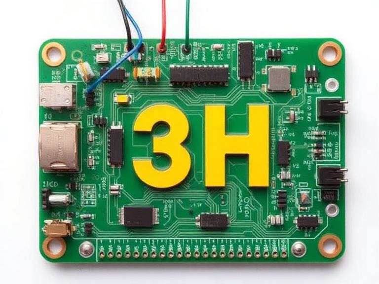
The 3H rule in PCB layout dictates that the minimum edge-to-edge distance between adjacent high-speed signal traces should be at least three times the height (H) of the dielectric material separating the routing layer from its nearest reference ground or power plane. By maintaining this 3H spacing, designers suppress electric field fringing and reduce mutual capacitance, effectively isolating sensitive signals from aggressive noise sources.
What It Is: The Understanding of the 3H Rule in PCB Layout
At its core, the 3H rule is an empirical layout guideline used to mitigate crosstalk in high-speed digital and radio frequency circuits. Here, "H" represents the vertical distance (height) between the conductive signal trace and the adjacent reference plane (usually a continuous copper ground or power plane). When two high-frequency traces run parallel across a board, changing electromagnetic fields induce currents from one conductor into the other. If the dielectric core or prepreg layer separating the trace layer from the ground plane is thick, the electric field lines spread out wider, increasing coupling.
For beginners encountering high-speed layout guidelines for the first time, this can feel abstract. However, when you are designing a high-performance High-Frequency PCB or a sensitive Radio Frequency PCB, ignoring dielectric height calculations results in corrupted packets and failed EMC compliance testing. The 3H rule provides a simple, highly effective geometric threshold to keep mutual coupling below critical thresholds.
How It Works: The Physics of Electric Fields and Dielectrics
To appreciate why the 3H rule works, we must examine how transmission lines interact with their reference planes. When a signal propagates down a trace, return currents flow through the reference plane directly underneath. The electric field lines extend from the trace down to the plane. The spread of these field lines is directly proportional to the dielectric height (H).
In our testing of dense Multilayer PCB assemblies, we observe that when a signal layer is located far from its reference plane—such as in asymmetrical stackups or thick core configurations—the electric field expands outward. If an adjacent trace enters this expanded field zone, capacitive coupling spikes. By enforcing a spacing of at least 3 times the dielectric height ($3 \times H$), designers ensure that over 70% to 80% of the electric field is successfully contained and returned to the reference plane rather than coupling laterally into neighboring traces.
This principle becomes even more vital when dealing with complex infrastructure like a high-density Backplane PCB, where high pin counts and dense routing channels test the absolute limits of physical separation.
Commercial and Performance Benefits
Implementing the 3H rule yields immediate, measurable improvements in board performance and commercial viability:
Significant Crosstalk Suppression: Drastically reduces near-end and far-end crosstalk between parallel high-speed data buses and clock lines.
Improved EMC Compliance: Prevents unintentional antenna effects and radiated emissions, ensuring your hardware passes FCC and CE regulatory testing on the first try.
Signal Integrity Preservation: Maintains clean eye diagrams, eliminates jitter, and prevents data packet corruption in high-speed communication links.
Reduced Respin Costs: Catching layout spacing errors prior to manufacturing saves thousands of dollars in prototype fabrication expenses.
Limitations and Practical Sourcing Realities
We must apply commercial and practical judgment: the 3H rule is a powerful heuristic, but it is not an absolute law of physics. Its primary limitation is board real estate. In ultra-dense mobile devices or compact IoT modules, maintaining a 3H clearance between every single trace is physically impossible.
Furthermore, the effectiveness of the 3H rule depends heavily on the integrity of your reference plane. If a high-speed trace crosses a split or a void in the ground plane, the return current is forced to detour, completely invalidating standard dielectric height assumptions. In heavy-duty applications requiring specialized material builds—such as a Heavy Copper PCB handling massive thermal and electrical loads—stackup geometries must be co-designed with your manufacturer to ensure dielectric constants ($D_k$) and layer heights support your spacing constraints.
Who Should Use It & Who Does Not Need It
For commercial users and high-speed designers: If you are routing DDR memory interfaces, gigabit Ethernet lines, PCIe lanes, or RF transceivers where signal edge rates are exceptionally fast (rise times under 1 nanosecond), applying the 3H rule (alongside its companion 3W rule) is non-negotiable. It protects your product against intermittent field failures.
Who does not need it: If you are designing low-speed microcontroller boards, simple LED drivers, or DC-DC power supply breakout boards operating at audio or low DC frequencies, strict adherence to the 3H rule is unnecessary overhead. Routing density should take priority when electromagnetic coupling is physically negligible.
Common Mistakes in High-Speed Routing
From our experience reviewing customer layout packages, engineering teams routinely commit three critical errors regarding spacing rules:
Confusing the 3H Rule with the 3W Rule: The 3W rule dictates that trace spacing should be 3 times the trace width (W) to manage magnetic field coupling. The 3H rule focuses on dielectric height (H) to manage electric field coupling when layers are distant from reference planes. Conflating the two leads to under- or over-engineered layouts.
Ignoring Stackup Variations Across the Board: Calculating 3H spacing based on an internal core height while routing on an outer prepreg layer with a completely different dielectric thickness. Always calculate H specifically for the exact layer pair in question.
Failing to Coordinate with Fabrication Limits: Pushing trace spacing so wide to satisfy 3H that it violates minimum trace-to-trace clearance capabilities of your board house, leading to manufacturing holds.
Fabrication and Sourcing Considerations
When preparing your layout for production, your choice of manufacturer directly impacts how successfully your high-speed design translates to physical copper. Consider these critical parameters:
Controlled Impedance Verification: Ensure your fabricator performs TDR (Time-Domain Reflectometry) testing to verify that dielectric heights match your simulation stackup.
Surface Finish Selection: For high-frequency wire bonding or fine-pitch surface mount components, specify a flat, high-reliability finish like ENIG(Electroless Nickel Immersion Gold)PCB to prevent skin-effect signal attenuation.
Full Process Traceability: Partner with a manufacturer who controls the entire production chain from inner-layer etching to final electrical testing.
Expert Recommendation from China 365PCB
In most professional situations, treating high-speed design rules as mere suggestions will result in costly board respins. We recommend establishing strict clearance constraints in your ECAD tool early in the design phase, mapping every high-frequency layer against its exact reference plane dielectric height.
As a fully self-operated, full-industry-chain manufacturing group, China 365PCB brings over 15 years of industry expertise across more than 100,000 square meters of self-owned production facilities. From advanced PCB fabrication and high-precision SMT assembly to online electronic component sourcing, CNC machining, and complete OEM/ODM solutions, we ensure total quality control and full process traceability. Whether you are fabricating complex multi-layer boards or specialized high-frequency builds, partnering with China 365PCB guarantees that your engineered stackups and spacing rules are executed with absolute manufacturing precision.
Data Analysis and Comparison Tables
Quick Summary Table: Core Parameters of the 3H Rule| Parameter | Engineering Definition | Primary Purpose |
|---|
| H (Dielectric Height) | Vertical distance from the trace layer to the reference ground/power plane. | Defines the expansion boundary of the trace's electric field. |
| 3H Spacing | Minimum edge-to-edge distance of 3 times the dielectric height. | Isolates adjacent traces to suppress capacitive crosstalk. |
| Applicable Signal Type | High-frequency digital buses, clocks, RF lines, fast edge-rate signals. | Minimizes EMI and maintains signal integrity across layers. |
Comparison Table: The 3H Rule vs. The 3W Rule| Comparison Metric | The 3H Rule | The 3W Rule |
|---|
| Core Variable | Dielectric Height (H) from reference plane. | Trace Width (W) of the conductor itself. |
| Primary Field Addressed | Electric field coupling and reference plane distance. | Magnetic field coupling between adjacent copper tracks. |
| Spacing Measurement | Edge-to-edge distance based on substrate thickness. | Center-to-center distance based on trace geometry. |
| Ideal Scenario | Thick core stackups or layers distant from ground planes. | Standard surface-layer parallel trace routing. |
Pros and Cons Table: Applying the 3H Rule| Pros (Advantages) | Cons (Limitations) |
|---|
| Effectively isolates sensitive high-speed nets from noise. | Consumes valuable routing channel real estate on dense boards. |
| Reduces electromagnetic radiation and aids EMC certification. | Requires precise stackup data from your PCB fabricator. |
| Simple geometric heuristic easy to implement in EDA tools. | May be impractical to enforce across 100% of ultra-dense BGAs. |
| Prevents costly hardware respins caused by signal corruption. | Does not eliminate crosstalk if reference planes contain splits. |
Buying Guide: Choosing Stackups for High-Speed Design| Design Complexity | Recommended Stackup Strategy | Key Engineering Priority |
|---|
| Standard 4-Layer Board | Signal-Ground-Power-Signal | Keep internal dielectric thin so outer traces maintain close reference coupling. |
| Complex 8+ Layer Multilayer | Alternating Microstrip/Stripline with dedicated Ground planes | Enforce strict 3H and 3W spacing rules on all critical high-speed differential pairs. |
| High-Power / Thermal Board | Heavy Copper internal planes with controlled prepreg thickness | Balance current-carrying copper weight with required high-frequency dielectric spacing. |
Frequently Asked Questions
What is the 3H rule in PCB design?
The 3H rule dictates that the edge-to-edge spacing between high-frequency signal traces should be at least three times the height (H) of the dielectric substrate separating the signal layer from the reference ground plane.
Why is the 3H rule important for high-speed signal integrity?
It helps minimize electromagnetic interference (EMI) and mutual inductive and capacitive coupling (crosstalk) by ensuring that electric field lines returning to the reference plane are adequately isolated between adjacent conductors.
How does the 3H rule differ from the 3W rule?
The 3W rule focuses on trace width (W) relative to center-to-center spacing to control magnetic field coupling, whereas the 3H rule focuses on dielectric height (H) to control electric field fringing and coupling when traces are located far from reference planes.
Authoritative References & Standards
To deepen your understanding of high-speed signal integrity and PCB design standards, consult these authoritative organizations:
David Li
David Li is the Technical Communications Director at China 365PCB, with over 15 years of hands-on experience in the PCB and electronics manufacturing industry. Holding a Master’s degree in Electrical Engineering, he has worked extensively in both R&D and manufacturing roles at leading multinational electronics firms in Shenzhen before joining our team.
His expertise spans high-speed digital design, advanced packaging (HDI, Flex), and automotive-grade reliability standards. David is passionate about bridging the gap between design intent and production reality—a philosophy that aligns perfectly with 365PCB’s mission to deliver seamless, rapid, and fully-integrated manufacturing solutions.
Follow David’s insights on PCB technology trends and best practices here on the 365PCB Knowledge Hub.
 English