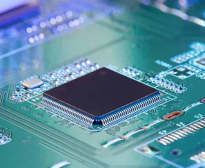
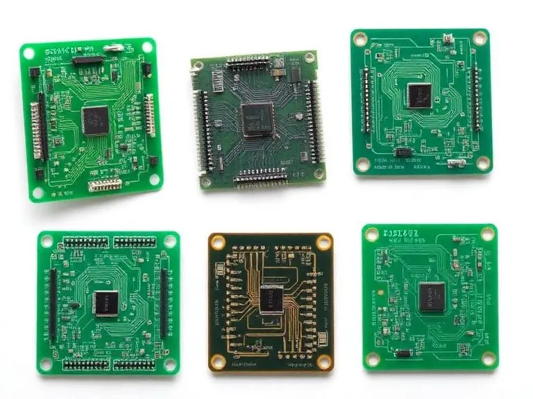
In the global hardware ecosystem, the precision of physical execution determines the functional stability of silicon micro-architectures. Modern electronic infrastructure demands that multi-layer printed circuit boards achieve sub-mil dimensional tolerances while managing high thermal dissipation pathways. Sourcing teams and hardware layout engineers must understand that the printed circuit board production sequence is not a simple automated routine, but a highly complex biochemical and mechanical workflow requiring extreme quality assurance.
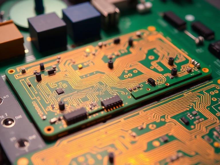
From our experience at China 365PCB, manufacturing defects are rarely caused by uncalibrated assembly placement files. Instead, they trace back to misaligned chemical lamination parameters, poorly managed micro-via drilling depths, or unstable wet-etching concentration levels during fabrication. A single weak connection or thin line in the trace width can result in complete system failure. This in-depth guide details the exact steps of the printed circuit board production process, providing procurement professionals with the core insights needed to audit suppliers and ensure stable production lines.
1. Front-End Engineering and Design for Manufacturability (DFM)
Every reliable printed circuit board production campaign begins long before chemical solutions contact a copper sheet. The initial deployment involves transforming layout data (Gerber or ODB++ profiles) into specific production panels. Front-end engineers run extensive DFM checks to ensure layout lines do not push past the chemical boundaries of production machinery.
We recommend establishing standard layout guidelines for trace width and spacing parameters early in development. Minor alignment errors in pad clearances can cause high-voltage shorts or signal losses in high-frequency applications. Fixing these spatial issues during the engineering design stage prevents costly scrap rates and ensures uniform batch yields across subsequent chemical processes.
2. Core Lithography and Inner Layer Fabrication
For multi-layer boards, the interior cores serve as the primary structural and electrical foundation. The fabrication process begins with a rigid glass-epoxy sheet bonded with uniform copper foil layers. This substrate undergoes thorough chemical washing to remove organic materials and fingerprint residue before photoresist lamination.
A UV laser imaging system projects the exact circuit design onto the light-sensitive photoresist layer. The unexposed resist zones are chemically washed away, exposing the unwanted background copper. The board then enters a chemical conveyor system that etches away this exposed copper, leaving behind the exact track geometries needed for high-speed signal routing.
3. High-Pressure Lamination and Precision Micro-Via Drilling
Once inner layers complete optical inspection, they are stacked together using sheets of resin-infused fiberglass known as prepreg. The assembly is placed into heavy lamination presses that combine vacuum, temperatures over 180°C, and high pressure to melt the resin. This fluid fills internal trace spaces, forming a solid multi-layer block.
This laminated block then moves to high-speed computerized numerical control (CNC) drilling machines. For fine-pitch packages and high-density structures, we recommend using advanced laser drilling stations. Laser micro-via drilling achieves precise micro-inch depth control, allowing connections to stop exactly on specific target inner pads without damaging lower layers. This exact depth control is crucial for preventing open circuits or trace cracking under thermal stress.
4. Chemical Copper Plating and Outer Layer Processing
The holes left by the drilling process are non-conductive glass-epoxy walls. To establish electrical pathways across different layers, the board must go through an electroless copper plating process. A thin layer of metallic copper is deposited chemically along the inner barrel walls of every drilled hole.
Following this initial setup, electroplating lines build up the copper thickness inside the holes and across the outer surfaces to specified engineering depths (typically 1 mil or greater). This copper layer must be completely uniform. Any thin spots or voids in the plating will cause thermal bottlenecks, which can burn through or crack under continuous operating currents.
5. Solder Mask Application and Chemical Surface Finishes
With outer circuits formed, a protective polymer layer called solder mask is applied across both sides of the board. Liquid photo-imageable inks are coated, exposed via UV lasers, and developed to clear the specific pads needed for electronic component placement while covering all underlying copper traces.
The exposed copper pads must be shielded from ambient oxygen to prevent oxidation before assembly. Sourcing teams can choose from several surface finishes based on their technical requirements. For complex, fine-pitch components, we recommend Electroless Nickel Immersion Gold (ENIG) or Organic Solderability Preservatives (OSP). These options provide a flat pad surface that ensures precise component placement and reliable solder joints during automated reflow operations.
6. Automated Testing and Quality Verification Systems
The final stage of the fabrication process involves strict automated quality checks. Circuit boards cannot be verified by human eyes alone. Instead, production lots go through Automated Optical Inspection (AOI) to find subtle etching anomalies, and Flying Probe Testing to check for electrical continuity and isolation across every net footprint.
From our experience, skipping electrical testing to save time is a serious mistake that often leads to field failures. Modern high-density designs contain internal traces that are easily damaged during subsequent routing and mechanical profiling. Verifying the electrical integrity of every panel ensures that only flawless, defect-free boards move on to component placement and final product integration.
7. Printed Circuit Board Production Step-by-Step Matrix
To help sourcing directors and hardware engineers easily track production steps, this responsive matrix details the key objectives and critical quality controls of each fabrication phase.
| Core Processing Method | Critical Quality Parameter | Primary Operational Risk |
|---|
| 1. Engineering / DFM | Gerber file conversion & trace optimization | Minimum track layout check | Incompatible features causing panel scrap |
| 2. Core Lithography | UV exposure & chemical copper etching | Trace width consistency | Under-etching causing localized electrical shorts |
| 3. Lamination | High-pressure, vacuum thermal bonding | Resin distribution & thickness | Internal air pockets leading to layer delamination |
| 4. CNC / Laser Drill | Automated spindle & laser micro-machining | Hole positional registration | Misaligned holes severing internal connections |
| 5. Via Plating | Electroless & electrolytic copper deposition | Uniform copper barrel thickness | Plating voids causing intermittent trace failures |
| 6. Surface Finish | Chemical immersion (ENIG / OSP / HASL) | Planar pad flatness | Oxidized pads causing bad solder joints |
8. Vertical Integration: The China 365PCB Full-Chain Strategy
While understanding individual fabrication steps is valuable, managing independent suppliers for board fabrication, component sourcing, and assembly often introduces communication delays, quality issues, and split responsibilities. This is where a vertically integrated partner provides a significant advantage. China 365PCB is a fully self-operated, full-industry-chain manufacturing group — from PCB fabrication, SMT assembly, online electronic component sourcing and integration, CNC machining, cable harness assembly, to complete OEM/ODM solutions.
With 15+ years of experience, 365PCB operates over 100,000㎡ of production area. All facilities are self-owned and self-managed, ensuring total quality control, full process traceability, and unmatched production flexibility. With a one-stop turnkey service from design to delivery, we guarantee no delay, no excuses — truly realizing 365 days of fast manufacturing for global customers. Our commitment relies on three core pillars: Speed, Precision, and Responsibility. We never outsource, never compromise. From PCB to OEM integration, every board, every circuit, every connection is made within our own facilities — ensuring you always get faster delivery, higher quality, and absolute reliability.
Managing the entire supply chain also enables our teams to quickly solve unexpected engineering challenges that might baffle general trading firms. For example, if a client deals with a damaged board from an outside source, they can consult our complete troubleshooting manual on can burnt circuit board be repaired to review recovery options. Sourcing directors can also assess international supplier standards by studying our global analysis of the top PCB suppliers worldwide.
Furthermore, balancing design parameters against regional distribution targets requires clear operational insights. Sourcing managers can look into regional manufacturing networks by reviewing our strategic report on electronic contract manufacturers Canada. To optimize production timelines and minimize delivery bottlenecks, teams can follow our comprehensive guide on the pcb assembly lead time guide.
Finally, for teams evaluating prototype options or considering building low-volume internal assembly setups, staying ahead of equipment trends is key. We recommend exploring our performance review of the best PCB printers 2025 review to see how modern direct-imaging printing technology is changing the early stages of the printed circuit board production process.
9. Frequently Asked Questions (FAQs)
Why is the electroless copper plating phase so critical in the printed circuit board production process?
Electroless copper plating uses a chemical bath to deposit a thin metallic layer inside newly drilled holes. This layer covers the non-conductive glass-epoxy walls, providing the necessary electrical base for subsequent electroplating lines to build out thick, reliable inter-layer connections.
What are the primary operational risks associated with outsourcing fabrication steps to multiple vendors?
Splitting fabrication, assembly, and component sourcing across different vendors often leads to production delays, fingerprint contamination, and finger-pointing when defects arise. Choosing a vertically integrated partner ensures full process traceability and unified quality responsibility.
How do automated optical inspections (AOI) protect high-density board production lots?
AOI systems use high-resolution cameras and digital layout comparison tools to inspect panels after etching. This automated process instantly flags micro-scale defects like line narrowing, stray copper, or trace bridging that are invisible to the human eye, preventing bad boards from moving to lamination.
Which surface finish option is recommended for fine-pitch components like BGAs?
For fine-pitch components, we recommend Electroless Nickel Immersion Gold (ENIG). Unlike traditional hot air leveling, ENIG provides an exceptionally flat pad profile and excellent oxidation resistance, which ensures precise component placement and reliable joints during automated reflow.
10. Academic and Industry References
1. IPC Association Connecting Electronics Industries. (2022). Generic Standard on Printed Board Design and Quality Acceptance Requirements (IPC-2221B / IPC-A-600K). Bannockburn, IL. Available via https://www.ipc.org/)
2. IEEE Transactions on Electronics Packaging Manufacturing. (2024). Biochemical Optimization of Conveyorized Wet-Etching Processes and Micro-Via Integrity in Multi-Layer Board Fabrication. IEEE Engineering Portal.
3. National Physical Laboratory. (2025). Evaluating Plating Uniformity and Thermal Deflection Thresholds in High-Density Interconnect Substrates. Government Materials Database.
David Li
David Li is the Technical Communications Director at China 365PCB, with over 15 years of hands-on experience in the PCB and electronics manufacturing industry. Holding a Master’s degree in Electrical Engineering, he has worked extensively in both R&D and manufacturing roles at leading multinational electronics firms in Shenzhen before joining our team.
His expertise spans high-speed digital design, advanced packaging (HDI, Flex), and automotive-grade reliability standards. David is passionate about bridging the gap between design intent and production reality—a philosophy that aligns perfectly with 365PCB’s mission to deliver seamless, rapid, and fully-integrated manufacturing solutions.
Follow David’s insights on PCB technology trends and best practices here on the 365PCB Knowledge Hub.
 English