Electromagnetic Interference (EMI) is the silent killer of modern electronics. As microprocessors push into multi-gigahertz operational speeds and form factors shrink, controlling radiated emissions is no longer optional—it is a strict regulatory requirement. For decades, one specific design guideline was treated as absolute gospel to combat this problem: the 20h rule in PCB design.
However, from our experience at China 365PCB, where we operate over 100,000 square meters of production area and handle everything from Custom PCB prototyping to massive OEM solutions, we see engineers blindly applying legacy rules that actively harm their modern designs. The electronics manufacturing industry is plagued by outdated "rules of thumb" that were formulated in the 1990s for slow-edge-rate, thick-dielectric boards.
In this comprehensive guide, we will take a definitive stance on the 20h rule in PCB layout. We will dissect what it is, the physics behind how it is supposed to work, and most importantly, whether it is actually worth using in your current hardware projects. We prioritize helping you make informed design and manufacturing decisions, avoiding costly redesigns and failed EMI compliance tests.
Quick Answer: The 20H Rule Explained
The 20h rule in PCB design states that the physical edge of a power plane should be recessed (pulled back) from the edge of the adjacent ground plane by a distance equal to 20 times the dielectric thickness (H) between them.
Is it worth using today? No. In most professional situations involving modern high-speed, high-density interconnect (HDI) designs, we strongly advise against it. Shrinking the power plane wastes critical board real estate, reduces inter-plane capacitance, and can inadvertently shift the board's resonant frequencies into a problematic spectrum, ultimately worsening EMI. Modern best practices dictate the use of ground stitching vias or edge plating instead.
What is the 20H Rule in PCB?
To understand the 20h rule in PCB architecture, you must first understand the fundamental layer stackup of a multilayer printed circuit board. In a typical configuration, a power plane (VCC) is placed directly adjacent to a ground plane (GND), separated only by a thin layer of non-conductive dielectric material (FR4, polyimide, etc.).
The letter H represents the height, or thickness, of that specific dielectric layer. The rule dictates that the copper boundary of the power plane should be etched away so that it sits entirely within the footprint of the ground plane. The setback distance must be exactly 20 multiplied by H. For example, if the dielectric thickness is 5 mils (0.127mm), the power plane must be pulled back 100 mils (2.54mm) from the edge of the ground plane.
How It Works: The Theory of Fringing Fields
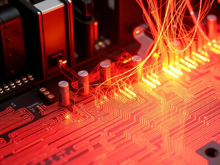
When high-frequency alternating currents travel through the power and ground planes, electromagnetic energy does not stay perfectly confined between the two copper layers. At the physical edge of the board, the electromagnetic field lines bulge outward into free space before curving back to terminate on the opposite plane. This phenomenon is known as fringing fields.
If these fringing fields radiate outward past the edge of the PCB, the board effectively acts as a patch antenna, broadcasting EMI and failing strict FCC or CE emission tests. The theory behind the 20h rule in PCB design is that by pulling the power plane back by a factor of 20H, the fringing fields are forced to terminate entirely on the overhanging edge of the ground plane, thereby absorbing the radiation before it escapes into the environment.
Quick Summary Table: The 20H Rule Mechanics| Variable | Definition | Impact on Design |
|---|
| H (Height) | Dielectric thickness between Power and Ground planes. | Determines the multiplier. Thicker dielectrics require massive, impractical pullbacks. |
| 20x Multiplier | The theoretical distance required to capture 70% of fringing flux. | Forces the power plane to be significantly smaller than the physical board outline. |
| Fringing Field | Electromagnetic flux bulging at the board edge. | The primary source of edge-radiated EMI that the rule attempts to mitigate. |
Historical Benefits: Why Was It Taught?
It is important to acknowledge that the 20h rule in PCB layout was not fabricated out of thin air. In the 1990s, when clock speeds were slower (sub-100MHz) and dielectric layers were substantially thicker (often 10 to 20 mils), this physical pullback genuinely helped mitigate a portion of radiated emissions.
For beginners learning legacy design, the rule provided a simple, mathematical heuristic to address a highly complex physics problem. It offered a sense of security for designers who lacked access to expensive 3D electromagnetic simulation software. In a thick-board, slow-signal environment, implementing the 20h rule in PCB architecture did absorb some fringing fields without causing catastrophic side effects.
Critical Limitations in Modern Designs
In our testing, and according to leading industry experts in signal integrity, the 20H rule completely falls apart in modern, high-speed digital designs. The physics of electromagnetic propagation change drastically as signal rise times drop below 1 nanosecond and frequencies push into the gigahertz spectrum.
First, pulling back the power plane reduces the physical area of parallel copper, which directly decreases the inter-plane capacitance. In high-speed designs, inter-plane capacitance is vital for Power Integrity (PI), acting as a high-frequency decoupling capacitor. Sacrificing this capacitance degrades your power delivery network.
Second, and more dangerously, altering the size of the power plane changes the resonant cavity dimensions of the PCB. In most professional situations today, we find that implementing the 20h rule in PCB layouts actually shifts the board's resonant frequencies higher, causing the board to radiate more EMI at specific high-frequency harmonics than if the planes were simply left flush.
Who Should Use It & Who Does Not Need It
For beginners and hobbyists: If you are designing a simple 2-layer or 4-layer through-hole board with a slow microcontroller (like an Arduino) and very thick prepreg layers, applying the rule won't hurt, but it is largely unnecessary.
For commercial users and heavy-duty applications: If you are designing a Consumer Electronics PCB, a dense Telecommunication PCB, or any HDI board with fast rise times, you absolutely do not need the 20h rule in PCB layout. In fact, utilizing it is detrimental. You are wasting critical routing space on miniaturized boards where every millimeter counts.
Common Mistakes in Applying the Rule
When clients submit Gerber files for our PCB Design Support Services, we frequently see the 20h rule in PCB layouts misapplied, leading to severe signal integrity issues.
Routing over the pullback gap: The most catastrophic mistake is pulling back the power plane, and then routing a high-speed signal trace over that newly created void on an adjacent signal layer. This destroys the return path, creating a massive impedance discontinuity and generating intense EMI.
Miscalculating board area: Designers often shrink the power plane so much that they cannot properly supply voltage to edge-mounted components, forcing them to use narrow power traces that create voltage drop (IR drop) issues. If you are calculating your PCB Actual Board Area (AOI) for assembly, ensure your power delivery reaches the components.
Pros and Cons Table: The 20H Rule| The 20H Rule in PCB | Pros (Theoretical) | Cons (Practical Reality) |
|---|
| EMI Mitigation | May reduce fringing fields on very specific, thick, slow-speed boards. | Can shift resonant frequencies, causing worse EMI at higher harmonics. |
| Power Integrity | None. | Reduces inter-plane capacitance, degrading the power delivery network. |
| Space Utilization | None. | Wastes critical board real estate at the perimeter of the PCB. |
Buying & Manufacturing Considerations
When deciding whether to implement the 20h rule in PCB architecture, you must factor in the manufacturing cost. Board real estate directly translates to financial cost. If you shrink your power plane by 100 mils on all sides, you are artificially restricting where you can place components and route power. This forces you to either increase the overall physical size of the PCB or add additional routing layers—both of which significantly drive up your fabrication costs during High-Volume Production PCB runs.
Instead of relying on outdated geometry rules, invest in modern manufacturing solutions. For instance, if EMI is a strict concern, passing the board through our PCB Electrical Testing Service and utilizing edge-plating (where the manufacturer plates the physical outer edge of the board with copper and ties it to ground) creates a literal Faraday cage that is infinitely superior to the 20H pullback.
Comparison Table: 20H Rule vs. Modern EMI Alternatives| Strategy | Mechanism of Action | Cost Impact | Verdict for 2026 |
|---|
| 20H Rule | Pulls power plane back to trap fringing fields. | Increases board size / wastes routing area. | Obsolete. Do not use for high-speed designs. |
| Via Stitching (Faraday Wall) | Placing a perimeter of ground vias along the board edge. | Negligible. Standard drilling process. | Highly Recommended. Excellent for shielding edge emissions. |
| Edge Plating (Castellation) | Wrapping the physical edge of the PCB in grounded copper. | Moderate premium (requires specialized routing/plating). | Best for extreme RF/EMI. Complete edge containment. |
Expert Recommendation from China 365PCB
From our experience as a full-industry-chain manufacturing group: Stop using the 20h rule in PCB design for modern hardware. It is a legacy myth that causes more problems than it solves in today's high-density electronics.
We recommend that commercial engineers maintain flush power and ground planes to maximize inter-plane capacitance and preserve routing real estate. If you are struggling with edge-radiated emissions, utilize a perimeter "picket fence" of ground stitching vias spaced at 1/20th of the wavelength of your highest harmonic frequency. This modern approach is structurally sound, highly effective, and easily executed within our 100,000㎡ self-managed fabrication facilities.
Frequently Asked Questions (FAQ)
Should I use the 20h rule in PCB design today?
In most professional situations today, no. The 20h rule in PCB design is largely considered a legacy rule of thumb that wastes valuable board space and can actually worsen electromagnetic interference (EMI) at high frequencies by altering the board's resonant cavities.
What does the "H" stand for in the 20H rule?
The "H" stands for the height or thickness of the dielectric material separating the power plane from the adjacent ground plane. The rule suggests pulling the power plane back by 20 times this physical height.
What is a better alternative to the 20h rule in PCB for EMI reduction?
A significantly better alternative for commercial users is utilizing ground stitching vias (a Faraday cage wall) along the perimeter of the board, specifying edge plating during manufacturing, or utilizing embedded capacitance materials, rather than simply shrinking the power plane.
Authoritative References & Industry Standards
To further validate why the 20h rule in PCB design is considered obsolete for high-speed digital engineering, we reference the following authoritative organizations and technical literature:
David Li
David Li is the Technical Communications Director at China 365PCB, with over 15 years of hands-on experience in the PCB and electronics manufacturing industry. Holding a Master’s degree in Electrical Engineering, he has worked extensively in both R&D and manufacturing roles at leading multinational electronics firms in Shenzhen before joining our team.
His expertise spans high-speed digital design, advanced packaging (HDI, Flex), and automotive-grade reliability standards. David is passionate about bridging the gap between design intent and production reality—a philosophy that aligns perfectly with 365PCB’s mission to deliver seamless, rapid, and fully-integrated manufacturing solutions.
Follow David’s insights on PCB technology trends and best practices here on the 365PCB Knowledge Hub.
 English