Authored by the advanced engineering team at China 365PCB. As a national-level high-tech enterprise, China 365PCB is a fully self-operated, full-industry-chain manufacturing group. From PCB fabrication and SMT assembly to online electronic component sourcing, CNC machining, and complete OEM/ODM solutions, we operate over 100,000 square meters of self-owned production area. With over 15 years of experience, we guarantee no delay and no excuses—truly realizing 365 days of fast manufacturing for global customers. We never outsource, never compromise.
In the rapidly evolving landscape of modern electronics, the miniaturization of devices and the demand for dynamic mechanical movement have pushed traditional rigid circuit boards to their operational limits. To accommodate these complex geometric and kinematic requirements, hardware engineers rely heavily on flexible printed circuits. However, mastering the Flexible PCB manufacturing process requires profound metallurgical knowledge, precise chemical engineering, and flawless dimensional stability control. The margin for error when processing polyimide substrates measuring only micrometers in thickness is virtually non-existent.

From our experience operating a full-industry-chain manufacturing group, understanding the intricacies of the Flexible PCB manufacturing process is essential for procurement officers, hardware developers, and electrical engineers. A poorly executed manufacturing phase can lead to flex cracking, impedance mismatches, and catastrophic field failures. We recommend evaluating your manufacturing partner strictly on their internal capabilities and quality control protocols. In this comprehensive technical guide, we will dissect every phase of the Flexible PCB manufacturing process, analyze the core material sciences involved, and demonstrate how our turnkey solutions at China 365PCB ensure absolute reliability.
1. Critical Materials in the Flexible PCB Manufacturing Process
The foundation of a successful Flexible PCB manufacturing process begins entirely with raw material selection. Unlike standard FR4 materials used in rigid boards, flexible circuits require substrates and conductive layers that can withstand repeated dynamic bending cycles without fracturing.
The primary dielectric substrate used is Polyimide (PI). PI films offer exceptional thermal stability, chemical resistance, and excellent electrical insulating properties. When executing the Flexible PCB manufacturing process, engineers must choose between adhesive-based and adhesiveless laminates. We recommend adhesiveless copper-clad laminates (FCCL) for high-frequency and highly dynamic applications because they offer a thinner profile, superior dimensional stability, and eliminate the risk of adhesive smearing during the drilling phase.
Equally critical is the copper foil. The Flexible PCB manufacturing process predominantly utilizes Rolled Annealed (RA) copper rather than Electrodeposited (ED) copper. RA copper features a horizontal grain structure that overlaps, providing significantly higher flexibility and resistance to fatigue cracking during dynamic bending. Our analysis shows that improper copper grain orientation during layout is a leading cause of premature failure, which is why our DFM (Design for Manufacturing) review meticulously verifies grain direction prior to fabrication.
2. Step-by-Step Guide to the Flexible PCB Manufacturing Process
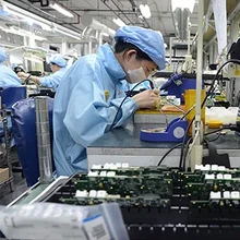
The Flexible PCB manufacturing process is highly sequential, requiring sterile cleanroom environments and automated handling equipment to prevent micro-creasing of the thin polyimide films. Below is the definitive workflow utilized in our 100,000 square meter production facility.
Step 1: Circuit Design, DFM Review, and Material Shearing

Before any physical fabrication begins, the Gerber data undergoes a rigorous DFM review. In the Flexible PCB manufacturing process, we must account for polyimide shrinkage. Polyimide naturally shrinks when subjected to etching and heat. We proactively apply scaling factors to the artwork to compensate for this dimensional shift. Once the digital files are approved, the roll-to-roll or paneled FCCL is sheared to specific production dimensions using high-precision automated cutters.
Step 2: CNC Drilling and Through-Hole Plating (PTH)
The panels are drilled using mechanical micro-drills or UV lasers for ultra-fine microvias. Because polyimide is flexible, specialized backing boards are utilized to prevent burring. Following drilling, the panels undergo a desmear process using a potassium permanganate plasma treatment to remove any melted resin from the hole walls. The panels then enter an electroless copper bath, depositing a microscopic layer of conductive copper inside the vias to establish electrical connectivity between the layers.
Step 3: Dry Film Lamination and Photolithography
The Flexible PCB manufacturing process proceeds to the cleanroom, where a photosensitive dry film is laminated onto the copper surface using heated rollers. The panel is exposed to ultraviolet light through a high-resolution photomask. The UV light polymerizes the dry film over the intended copper traces, hardening it. The unexposed film is then chemically developed and washed away, leaving the target copper exposed for the next stage.
Step 4: Acidic Etching and Stripping
The panels are passed through a highly controlled acidic etching chamber. The chemical solution dissolves the unprotected copper, leaving behind only the precise circuit traces protected by the hardened dry film. Once the etching is complete, the remaining dry film is stripped away using an alkaline solution, revealing the final copper circuitry. In the Flexible PCB manufacturing process, controlling the etch factor is paramount to ensuring accurate trace width and impedance values.
Step 5: Coverlay Alignment and Lamination
Unlike rigid boards that use liquid photoimageable solder mask, the Flexible PCB manufacturing process relies on a solid polyimide coverlay. The coverlay is pre-drilled to expose surface mount pads and is aligned perfectly over the etched circuitry. The assembly is placed in a vacuum lamination press. Under highly specific temperature and pressure profiles, the adhesive on the coverlay flows and encapsulates the copper traces, providing physical protection and dielectric insulation.
Step 6: Surface Finishing
To protect the exposed copper pads from oxidation and ensure excellent solderability during SMT assembly, a surface finish is applied. From our experience, the most reliable finish in the Flexible PCB manufacturing process is ENIG (Electroless Nickel Immersion Gold). It provides a highly planar surface ideal for fine-pitch components and offers excellent shelf life without compromising the flexibility of the board.
Step 7: Profiling, Laser Routing, and Electrical Testing
The final mechanical step involves extracting the individual flexible circuits from the production panel. Traditional routing routers can tear the fragile polyimide, so we utilize precision steel rule dies or high-speed UV laser profiling for complex geometries. Finally, every board undergoes automated optical inspection (AOI) and flying probe electrical testing to guarantee zero open or short circuits before shipment.
3. Engineering Challenges in the Flexible PCB Manufacturing Process
Mastering the Flexible PCB manufacturing process is notoriously difficult due to the inherent physical properties of the materials. The most prominent challenge is maintaining dimensional stability. As the material absorbs ambient moisture and undergoes thermal cycling during lamination, it expands and contracts. At China 365PCB, our environmental control systems maintain strict temperature and humidity parameters across the entire production floor to mitigate these shifts.
Another major challenge is maintaining signal integrity in high-speed applications. Creating controlled impedance traces on a flexible substrate requires absolute precision in dielectric thickness and trace width etching. This is why we never outsource. By maintaining total quality control within our own facilities, we ensure that the rigorous demands of the Flexible PCB manufacturing process are met with exact precision every single time.
4. Integrating Comprehensive PCB Services at China 365PCB
While the Flexible PCB manufacturing process is highly specialized, modern electronics often require hybrid architectures. At China 365PCB, we believe true manufacturing excellence lies in Speed, Precision, and Responsibility. Because we operate a fully self-operated, full-industry-chain manufacturing group, we seamlessly integrate our flexible circuit capabilities with our broader product portfolio.
Our comprehensive services include the fabrication of Rigid Flex PCB and Flex-Rigid Board structures, which combine the durability of standard FR4 with the dynamic capabilities of polyimide. Furthermore, our production lines are fully equipped to handle Metal Core PCB, ENIG(Electroless Nickel Immersion HDI) PCB, Radio Frequency PCB, Single Sided PCB, Heavy Copper PCB, Double Sided PCB, Aluminum PCB, High-Frequency PCB, and Multilayer PCB configurations.
From PCB fabrication to SMT assembly and complete OEM/ODM integration, every board, every circuit, and every connection is made within our own facilities. We guarantee you always get faster delivery, higher quality, and absolute reliability.
5. Summary Table: Flexible PCB Manufacturing Process Key Stages
| Process Stage | Engineering Objective | Quality Control Metric |
|---|
| DFM & Material Preparation | Scale artwork for polyimide shrinkage and select RA copper. | Grain orientation verification and dimensional scaling accuracy. |
| Laser Drilling & PTH | Create microvias and establish interlayer connectivity. | Plasma desmear validation and copper plating thickness. |
| Photolithography & Etching | Transfer circuit image and remove excess copper. | Trace width tolerance and impedance verification. |
| Coverlay Lamination | Encapsulate traces with polyimide for protection. | Vacuum pressure monitoring and void-free adhesion. |
| ENIG Surface Finish | Prevent copper oxidation and ensure solderability. | Nickel and Gold thickness measurement (XRF). |
| Laser Profiling & Testing | Extract final board and verify electrical continuity. | AOI accuracy and Flying Probe resistance values. |
6. Frequently Asked Questions (FAQs)
Why is RA copper preferred over ED copper in the Flexible PCB manufacturing process?
From our experience, Rolled Annealed (RA) copper possesses an elongated, overlapping grain structure that handles dynamic bending and physical stress vastly better than the vertical, columnar grain structure of Electrodeposited (ED) copper. Using RA copper drastically reduces the risk of trace fracturing in dynamic flex applications.
What is the difference between a standard Flexible PCB and a Rigid Flex PCB?
A standard flexible PCB consists entirely of flexible polyimide materials. A Rigid Flex PCB, which we expertly manufacture at China 365PCB, integrates rigid FR4 sections internally bonded to flexible layers. This allows for complex 3D assembly and component mounting on stable rigid areas while utilizing the flex sections to eliminate wire harnesses between boards.
How does China 365PCB ensure quality during the Flexible PCB manufacturing process?
We ensure total quality control because we never outsource. Our 100,000 square meter production facility is entirely self-owned and self-managed. By keeping the entire Flexible PCB manufacturing process under one roof—including SMT assembly and component sourcing—we guarantee full process traceability and uncompromising precision.
Can you handle high-frequency signals on a flexible substrate?
Yes. By utilizing specialized adhesiveless polyimide laminates, precise impedance control during the etching phase, and careful coverlay lamination, the Flexible PCB manufacturing process can easily accommodate High-Frequency PCB and Radio Frequency PCB requirements for aerospace and telecommunications applications.
7. Academic and Industry References
 English


