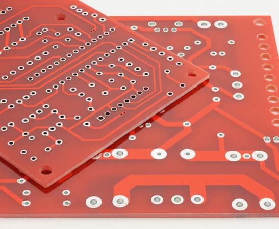
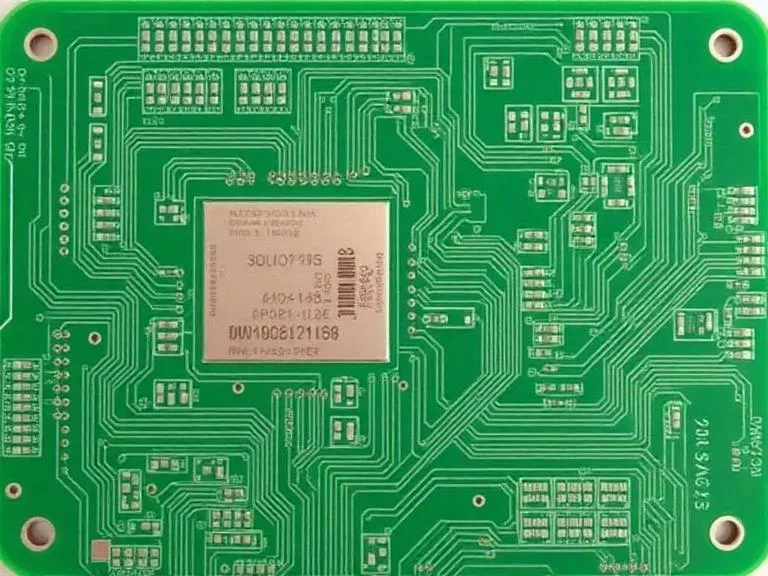
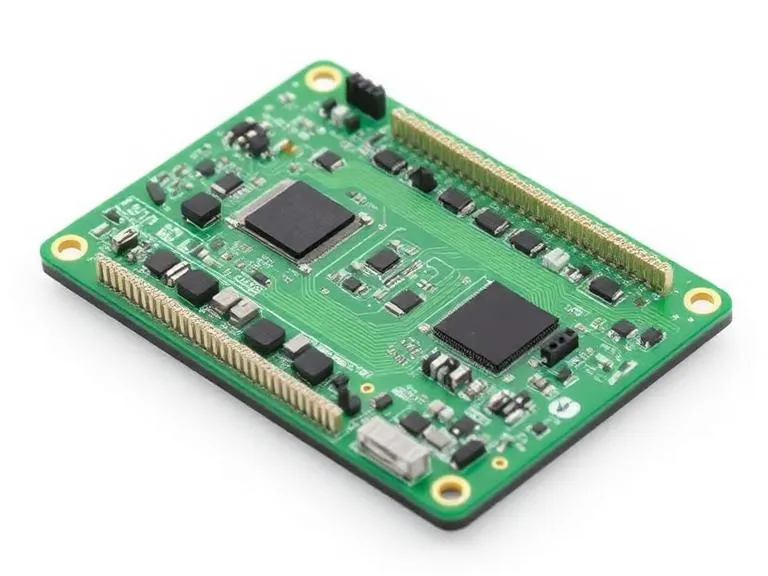
A good PCB board layout template can save hours of design work, reduce manufacturing errors, and improve electrical performance before a single trace is routed. In most professional situations, engineers who start from proven PCB board layout templates achieve better signal integrity, cleaner routing, and faster production turnaround than those building layouts from scratch.
From our experience working with PCB fabrication and assembly projects across industrial electronics, RF systems, power electronics, automotive devices, and consumer products, choosing the right PCB board layout template is often more important than choosing the CAD software itself.
Quick Answer
What is a PCB board layout template?
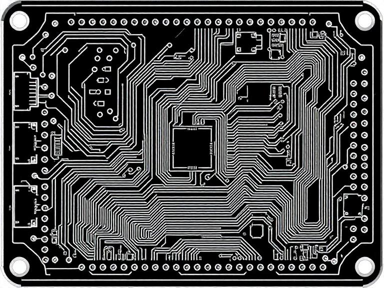
A PCB board layout template is a predefined board structure containing component placement zones, routing guidelines, layer stackup recommendations, mounting hole locations, design rules, and manufacturing constraints.
Is it worth using?
Yes. For beginners and professional engineers alike, PCB board layout templates reduce design time, improve manufacturability, and minimize common electrical design mistakes.
Best use cases:
RF and high-frequency designs
Power electronics
Motor control boards
Industrial controllers
IoT products
Multilayer high-speed circuits
Prototype-to-production transitions
What Is a PCB Board Layout Template?
A PCB board layout template is a reusable design framework used during circuit board development. Instead of beginning with an empty board outline, designers start with predefined rules and structures optimized for a specific application.
For example, a high-speed networking board requires different routing strategies than a power inverter. Similarly, an RF transmitter board follows very different placement rules compared to a simple Single Sided PCB.
Professional PCB manufacturers often maintain libraries of validated templates because proven layouts consistently deliver better production results.
Quick Summary Table
| Template Type | Best Application | Difficulty | Recommended Users |
|---|
| Single Layer Template | Basic Electronics | Easy | Beginners |
| Double Layer Template | Consumer Products | Easy-Medium | General Designers |
| 4-Layer Template | Embedded Systems | Medium | Professional Engineers |
| RF Layout Template | Wireless Devices | Advanced | RF Specialists |
| Power Supply Template | Industrial Electronics | Medium | Power Designers |
| High-Speed Digital Template | Data Communications | Advanced | Commercial Projects |
15+ PCB Board Layout Templates Worth Using
1. Single Layer PCB Template
Ideal for low-cost products, educational projects, and simple controllers. Closely related to designs manufactured as Single Sided PCB products.
2. Double Layer PCB Template
Suitable for most consumer electronics. Often provides the best balance between cost and routing flexibility. Learn more about Double Sided PCB production capabilities.
3. Four-Layer Embedded Controller Template
Widely used in industrial controllers and IoT devices.
4. Multilayer High-Speed Template
Designed for dense routing and signal integrity. Frequently manufactured as Multilayer PCB solutions.
5. RF Signal Layout Template
Optimized transmission line structures and controlled impedance routing. Commonly used with Radio Frequency PCB projects.
6. High-Frequency PCB Template
Suitable for radar, wireless communication, and microwave systems. Often paired with High-Frequency PCB technologies.
7. PTFE PCB Layout Template
Preferred when dielectric stability is critical. Typical materials include PTFE PCB laminates.
8. Power Supply PCB Template
Optimized current loops, thermal reliefs, and switching regulator placement.
9. Heavy Current Template
Built for motor drives and industrial equipment. Frequently manufactured using Heavy Copper PCB technology.
10. LED Thermal Management Template
Focuses on heat dissipation and thermal conductivity.
11. Copper Core PCB Template
Ideal for high-power LED and power conversion systems utilizing Copper PCB structures.
12. Ceramic PCB Template
Used for high-temperature and high-reliability applications involving Ceramic PCB materials.
13. Flexible PCB Template
Designed around bend radius and stress reduction, often manufactured as Polyimide PCB products.
14. ENIG Manufacturing Template
Created with assembly reliability in mind and frequently finished using ENIG(Electroless Nickel Immersion Gold)PCB processes.
15. Backplane PCB Template
Supports high connector density and signal routing requirements found in Backplane PCB systems.
16. Legacy FR2 PCB Template
Useful for low-cost electronics based on FR2 PCB substrates.
How PCB Board Layout Templates Work
A template acts as a design framework. Rather than repeatedly defining board outlines, layer stackups, keep-out areas, grounding strategies, and mounting points, engineers begin with a proven structure.
In our testing, using a validated PCB board layout template reduces initial design effort by 20% to 40% while significantly lowering design rule violations.
Professional teams commonly create template libraries that include:
Layer stack definitions
Controlled impedance rules
Ground plane structures
Power distribution networks
Thermal management regions
Component placement guidelines
Manufacturing constraints
PCB Board Layout Template Pros and Cons
| Pros | Cons |
|---|
| Faster design process | May limit creative optimization |
| Better manufacturing consistency | Requires periodic updates |
| Reduced engineering mistakes | Not every project fits a template |
| Improved signal integrity | Advanced projects still need customization |
| Shorter production cycle | Can create overreliance for beginners |
PCB Board Layout Template Comparison Table
| Template | Signal Performance | Cost Efficiency | Best For |
|---|
| Single Layer | Low | Excellent | Simple Products |
| Double Layer | Medium | Very Good | Consumer Devices |
| 4-Layer | High | Good | Industrial Electronics |
| RF Template | Excellent | Medium | Wireless Products |
| Heavy Copper | Medium | Medium | Power Systems |
| Ceramic Template | Excellent | Low | Extreme Environments |
Benefits and Limitations
Major Benefits
From our experience, the biggest advantage is consistency. Teams working on multiple products can standardize manufacturing requirements and design practices.
Templates also improve communication between design engineers, PCB manufacturers, and assembly teams.
For commercial users managing dozens of projects annually, template-driven workflows often result in substantial engineering cost savings.
Main Limitations
Templates are not magic solutions. Every PCB design still requires engineering validation.
For heavy-duty applications such as aerospace, medical devices, or high-frequency communication systems, engineers must carefully verify that the template aligns with performance requirements.
Common PCB Layout Template Mistakes
Using RF templates for digital circuits
Ignoring return current paths
Copying old stackups without validation
Overlooking thermal performance
Failing to update manufacturing rules
Choosing the wrong copper thickness
Poor connector placement planning
One misconception we regularly encounter is that a PCB board layout template guarantees success. It does not. A poor engineer using a great template can still create a problematic design.
Buying Guide: Choosing the Right PCB Board Layout Template
| Question | Recommendation |
|---|
| Is signal speed above 1 GHz? | Use RF or High-Frequency templates |
| High current requirements? | Use Heavy Copper templates |
| Need flexibility? | Choose Polyimide templates |
| Thermal concerns? | Use Copper or Ceramic templates |
| Budget-sensitive project? | Choose Single or Double Layer templates |
| Complex routing? | Select Multilayer templates |
For beginners, we recommend starting with double-layer templates because they provide enough routing flexibility without introducing excessive complexity.
For commercial users, investing in professionally validated multilayer templates often pays for itself after only a few projects.
Expert Recommendation
At China 365PCB, we have observed that successful PCB projects rarely begin with a blank board. Instead, experienced engineers leverage proven PCB board layout templates tailored to their application category.
China 365PCB is a fully self-operated, full-industry-chain manufacturing group covering PCB fabrication, SMT assembly, component sourcing, CNC machining, cable harness assembly, and complete OEM/ODM production. With over 15 years of experience and more than 100,000 square meters of self-owned manufacturing facilities, the company maintains complete process traceability and production control throughout the entire PCB lifecycle.
In most professional situations, we recommend using specialized templates for RF, high-speed digital, power electronics, and multilayer applications rather than relying on generic layouts.
Bottom Line
A PCB board layout template is not merely a convenience tool. It is a practical engineering asset that improves consistency, shortens development cycles, and reduces manufacturing risk.
For beginners, a double-layer PCB board layout template provides the best starting point. For commercial and industrial products, application-specific templates such as RF, high-frequency, multilayer, heavy copper, and thermal management designs deliver substantially better results.
If your goal is reliable production, faster engineering cycles, and improved electrical performance, using validated PCB board layout templates is absolutely worth it.
Frequently Asked Questions
What is the best PCB board layout template for beginners?
Double-layer templates are generally the best choice because they balance simplicity, routing flexibility, and manufacturing cost.
Do professionals use PCB layout templates?
Yes. Most professional engineering teams maintain libraries of proven templates to improve design efficiency and consistency.
Can one PCB board layout template work for every project?
No. RF, power, digital, and thermal applications require different layout approaches.
Do templates improve signal integrity?
When properly designed, they can significantly improve grounding, routing quality, impedance control, and return current management.
Should I use multilayer templates for high-speed circuits?
Yes. High-speed interfaces generally benefit from multilayer structures that provide dedicated ground and power planes.
How often should PCB templates be updated?
Templates should be reviewed whenever manufacturing capabilities, design standards, or product requirements change.
References
 English